
User’s
Manual for GAIN Program
Programmed
by Dr. Tso-min Chou
Manual Written by Photonic Study Group
Southern
Fall 2003

User’s
Manual for GAIN Program
Programmed
by Dr. Tso-min Chou
Manual Written by Photonic Study Group
Southern
Fall 2003
Table of Contents
Chapter 2 Computation of Material Composition and Band
Edges
2.1 Input Parameters for Each Material System
2.3 Running the Software for Material Composition and
Band Edge Calculations
2.3.1 Selecting the Material
System
Chapter 3 Energy Band Calculations
3.1 Brief Overview for Energy Band Calculations
3.2 Explanations on Input and Output Parameters
3.2.1 Calculating the Energy
Values
3.2.2 Inputting Structure
Parameters
3.2.3 Selecting the Material
System
3.2.5 Calculation of Energy
Values
3.2.6 Calculation of
Envelope Functions and Confinement Factors
3.4 Running the Software for Energy Calculations, an
Example
3.4.1 Conduction Band Energy
Calculations
3.4.2 Conduction Band Heavy
and Light Hole Band Energy Calculations
Chapter 4 Simulations of Gain and Laser Properties
4.1 Theories for computations of Gain and Laser
Properties
4.1.2 Threshold Current
Density (Jth) and Slope Efficiency Calculations
4.3.1 The table for the
Output Files.
4.3.2 The Drawings for the
Output Files.
4.4 Running the Software for Gain and Laser
Characteristics
Appendix A Material Parameters
1 AlGaAs/AlGaAs
(Substrate: GaAs)
2 InGaAsP/InGaAsP
(Substrate: InP)
3 InGaAs/InGaAsP/InP
(Substrate: InP)
4 InGaAlAs/InGaAlAs
(Substrate: InP)
5 GaInP/(AlGa)0.5In0.5P/AlInP
(Substrate: GaAs)
6 InGaAs/AlGaAs/AlGaAs
(Substrate: GaAs)
8 AlyInxGa1-x-yAs/AlzGa1-zAs/GaAs
(Substrate: GaAs)
9
InzGa1-zAs/AlxGayIn1-x-yAs/AlxGayIn1-x-yAs(Substrate:
InP)
10 InGaAlAs/InGaAlAs/AlAsxSb1-x (Substrate: InP)
11
Ga1-zAs/AlxGayIn1-x-yAs/AlAsxSb1-x (Substrate: InP)
12 In(y)Ga(1-y)As(x)N(1-x)/GaAs (dilute N) (Substrate
GaAs)
13
In(1-x)Ga(x)As(y)P(1-y)/GaAs (Substrate GaAs)
Appendix B Complex Structure Examples
B.1 A
1.55μm InGaAlAs/InP compressive strained Single-Quantum-Well laser with
GRIN structure
Appendix C Examples for Each Material System
The GAIN program is a software program that is used to
calculate the gain and r elated parameters in semiconductor quantum well laser structures.
This tool can be used mainly in optoelectronics and photonics fields. It is
free and runs under DOS and Windows based platforms.
The software works for thirteen material systems most of which are used to make semiconductor quantum well lasers, find the band offsets and energy levels in both conduction and valence bands, and calculate the gain curves with respect to wavelength and current density. The program uses one-dimensional analysis in computations, and gives fast and practically accurate results.
This software was developed by Dr. Tso-min Chou in the
Department of Electrical Engineering at Southern Methodist University,
The contributions in preparing this User’s Manual by the members of the Photonics Group at SMU are greatly appreciated.
This chapter includes the introduction of the input parameters for each material system and the output files generated by running the material system. The given example is for 1.55um single quantum well strain compensated SCH structure. For a better reading of this manual, the following conventions are used for giving the example of running the program. The Italic style is for the output screen from the screen of the program. The user’s typing starts with a “>” to indicate the user’s input.
There are four major kinds of input parameters (I, II, III, and IV) for each material system. The following paragraph explains each input parameters:
This is the number of the layers except for the quantum well. For example, the simple SCH quantum well structure has the “N” which equals to 2. For the graded index SCH structure with single quantum well that can have 10 steps between the quantum part and cladding part, we then need to give N equaling to 11. N-1 does not include the cladding layer. Figure 2.1.1 shows the different conduction band structure of the simple and graded index SCH.

Figure 2.1.1 Different SCH structure for band edge profile
The wavelength range differs with the material system. We give the wavelength range for each material system layer in appendix A. The QW wavelength has the highest wavelength, then barrier wavelength and then cladding because of the band gap difference for different layers. The wavelength in the QW is related to the desired lasing wavelength. However, the input wavelength is approximated according to the bulk material’s energy band gap. If the user know the composition for quantum well, barrier and cladding layer, the appendix A provides the formula to calculate the wavelength. The wavelength in um can be obtained from 1.24/energy band gap.
Users can input the desired width value in am-strong Å. If the GRINSCH and multiple quantum wells structure is for the desired structure, the user needs to be aware of the input value for the barrier width. The program divides the input barrier width over N-1 as the barrier width between the quantum wells.
From the strain constant (e) [1],
![]() (2.1)
(2.1)
where aq , ab are lattice constants of the quantum well and barrier layers, respectively. From energy band semiconductor structure, figure 2.1.2, we know that the value of tensile strain is positive for aq< ab, and compressive strain has a negative value for aq> ab. (2.1) is good for the unstrained barrier and the barrier is lattice matched to the substrate. In (2.1), we can always put aq as the strain layer and ab for unstrain layer, which is usually lattice match to the substrate, to calculate the strain. For example, if we put strain in the barrier, we will have the barrier lattice as aq and substrate lattice as ab.
The other definition is often used for the strain constant
![]() (2.2)
(2.2)
where au is the unstrained layer and usually lattice match to substrate, as is the strained layer
For this definition, as > au is compressive strain. We will get the positive strain constant. Similarly, if as < au, which is tensile strain, we will get the negative strain constant. However, for the Gain program, we use the equation (2.1) for the definition of the strain constant.
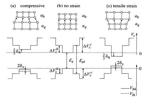
Figure 2.2.2 Energy band semiconductor structure. The conduction Vc and valence Vhh, Vlh potentials for a semiconductor structure with quantum-well, barrier and cladding layers. Notation: dh: hydrostatic potential, ds:shear potential, Eg: energy band gap for quantum well, Egb: energy band gap for barrier, DVcb: conduction band offsets for the barrier, DVcc: conduction band offsets for the cladding, DVvb: valence band offsets for the barrier, DVvc: valence band offsets for the cladding.
Different material systems may have slightly different input parameters and procedures. The only big variation is for material system #10, which does not need the wavelength and width input parameters. So a list of input parameters and steps for each material system is shown in Table 2.1 based on the order that they appear in program screen.
Table 2.1 Necessary input steps for each material system
|
Material |
Step 1 |
Step 2 |
Step 3 |
Step 4 |
|
(1)AlGaAs/AlGaAs |
# of GRIN |
QW wavelength |
Barrier wavelength |
Cladding wavelength |
|
(2)InGaAsP/InGaAs |
# of GRIN |
QW wavelength |
Barrier wavelength |
Cladding wavelength |
|
(3)InGaAs/InGaAsP/InP |
# of GRIN |
QW wavelength |
Barrier wavelength |
Cladding wavelength |
|
(4)InGaAlAs/InGaAlAs |
# of GRIN |
QW wavelength |
Barrier wavelength |
Cladding wavelength |
|
(5)GaInP/(AlGa)0.5In0.5P/AlInP |
# of GRIN |
QW wavelength |
Barrier wavelength |
Cladding wavelength |
|
(6)InGaAs/AlGaAs/AlGaAs |
# of GRIN |
QW wavelength |
Barrier wavelength |
Cladding wavelength |
|
(7)InGaAs/InGaAsP/Ga0.51In0.49P(MATCHED GaAs) |
# of GRIN |
QW wavelength |
Barrier wavelength |
Cladding wavelength |
|
(8)AlyInxGa1-x-yAs/AlzGa1-zAs/GaAs |
# of GRIN |
QW wavelength |
Barrier wavelength |
Cladding wavelength |
|
(9)InzGa1-zAs/AlxGayIn1-x-yAs/InP |
# of GRIN |
QW wavelength |
Barrier wavelength |
Cladding wavelength |
|
(10)InGaAlAs/InGaAlAs/AlAsxSb1-x(matched InP) |
Compress or Tensile |
J |
Strain |
|
|
(11)InzGa1-zAs/AlxGayIn1-x-yAs/AlAsxSb1-x |
# of GRIN |
QW wavelength |
Barrier wavelength |
Cladding wavelength |
|
(12)In(y)Ga(1-y)As(x)N(1-x)/GaAs (dilute N) |
# of GRIN |
QW wavelength |
Barrier wavelength |
Cladding wavelength |
|
(13)In(1-x)Ga(x)As(y)P(1-y)/GaAs |
# of GRIN |
QW wavelength |
Barrier wavelength |
Cladding wavelength |
Table 2.1 Necessary input steps for each material system (continued)
|
Material |
Step 5 |
Step 6 |
Step 7 |
|||||
|
(1)AlGaAs/AlGaAs |
Input C, B, QW width in Å |
|
|
|||||
|
(2)InGaAsP/InGaAs |
Input C, B, QW width in Å |
Input Ex |
Lattice matched barrier |
|||||
|
Strain compensated(then input strain Ex for
barrier) |
||||||||
|
(3)InGaAs/InGaAsP/InP |
Input C, B, QW width in Å |
Lattice matched barrier |
|
|||||
|
Strain compensated |
Input strain Ex for barrier |
|||||||
|
(4)InGaAlAs/InGaAlAs |
Input C, B, QW width in Å |
Input strain |
Choose Dr.Chuang or experimental |
Lattice match |
|
|||
|
Input strain |
Choose (1) or (2) |
|||||||
|
(5)GaInP/(AlGa)0.5In0.5P/AlInP |
Input C, B, QW width in Å |
AlGaInP lattice match to GaAs |
|
|||||
|
AlGaInP mismatch |
Input strain |
|||||||
|
(6)InGaAs/AlGaAs/AlGaAs |
Input C, B, QW width in Å |
|
|
|||||
|
(7)InGaAs/InGaAsP/Ga0.51In0.49P(MATCHED GaAs) |
Input C, B, QW width in Å |
Input wavelength for barrier |
|
|||||
|
(8)AlyInxGa1-x-yAs/AlzGa1-zAs/GaAs |
Input C, B, QW width in Å |
Input strain |
|
|||||
|
(9)InzGa1-zAs/AlxGayIn1-x-yAs/InP |
Input C, B, QW width in Å |
Lattice matched barrier |
|
|||||
|
Strain compensated |
Dr.Chuang’s |
Input strain |
||||||
|
Experimental |
||||||||
|
(10)InGaAlAs/InGaAlAs/AlAsxSb1-x(matched InP) |
|
|
|
|||||
|
(11)InzGa1-zAs/AlxGayIn1-x-yAs/AlAsxSb1-x |
Input C, B, QW width in Å |
|
|
|||||
|
(12)In(y)Ga(1-y)As(x)N(1-x)/GaAs (dilute N) |
Input C, B, QW width in Å |
Input strain |
|
|||||
|
(13)In(1-x)Ga(x)As(y)P(1-y)/GaAs |
Input C, B, QW width in Å |
Lattice matched barrier |
|
|||||
|
Strain compensated |
Input strain EX |
|||||||
Two output files – CBANDEG.DAT and VBANDEG.DAT will be generated after running the step of “FOR THE NECESSARY PARAMETERS” in GAIN program by inputting all the necessary parameters for the selected material system. In both files, the first row contains the strain and lattice constant of quantum well, the 1st, 2nd and 3rd column of the rest rows show the layer thickness, composition of x component, and composition of y component for each layer, respectively. The 4th column of CBANDEG.DAT gives conduction band offset for each layer while that of VBANDEG.DAT gives valance band offset for each layer.
The unit of layer thickness and lattice constant in both CBANDEG.DAT and VBANDEG.DAT is angstrom, and the unit of energy band offsets is electron volts (eV). The compressive-strained quantum well has a negative value of strain as opposed to the positive strain value of tensile-strained quantum well. The zero energy reference level for conduction band offset is non-strained quantum well bulk material conduction band edge, and the zero energy reference level for valance band offset is non-strained quantum well bulk material valance band edge. Therefore, as indicated by Figure 2.1.2, the quantum well conduction band offset is zero for non-strained quantum well, positive for compressive-strained quantum well and negative for tensile-strained quantum well. Vise versa for the valance band offset of the quantum well. The barrier and cladding band offsets are always positive for conduction band and negative for valance band.
If we use QW, BR, CL as acronyms of quantum, barrier and cladding, and assume that the material components for each layer has the general form of A(x)B(1-x)C(y)D(1-y) with A,B,C,D represent the arbitrary 4 material elements and x, 1-x, y, 1-y represent the compositions of A, B, C and D, use 5-layer symmetric structure as an example, the CBANDEG.DAT and VBANDEG.DAT have the general forms as shown below.
 QW_strain QW_lattice constant
CL thickness CL x-composition CL y-composition CL C-band offset
BR thickness BR x-composition BR y-composition BR C-band offset
QW thickness QW x-composition QW y-composition QW C-band offset
BR thickness BR x-composition BR y-composition BR C-band offset
CL thickness CL x-composition CL y-composition CL C-band offset
 QW_strain QW_lattice constant
CL thickness CL x-composition CL y-composition CL V-band offset
BR thickness BR x-composition BR y-composition CR V-band offset
QW thickness QW x-composition QW y-composition QW V-band offset
BR thickness BR x-composition BR y-composition BR V-band offset
CL thickness CL x-composition CL y-composition CL V-band offset
In this section, we show the details of how to run the GAIN program to calculate the material compositions and band edges. As shown in section 2.2, the output files, “cbandeg.dat” and “vbandeg.dat”, give the band gap, composition and layer thickness information.
After typing “GAINV1A” under the executable file directory from the DOS prompt or directly double click on the gain program executable file, the program will prompt the following:
****************************************************
THE MAIN PROGRAM IS ONLY A CALLING PROGRAM, WHICH
CONTAINS THREE MAJOR PARTS (MORE THAN 20 SUBROUTINES
FIRST SELECT MATERIAL PARAMETERS.
SECOND SELECT ENERGY LEVELS IN BOTH BANDS.
THIRD FIND THE G(J), G(WAVELENGTH) AND RATE EQUATIONS
****************************************************
MAKE YOUR SELECTION NOW!
ENTER 1 FOR THE NECESSARY PARAMETERS
2 FOR THE ENERGY VALUES OF CONDUCTION BAND
3 FOR THE ENERGY VALUES OF HEAVY HOLE BAND
4 FOR THE ENERGY VALUES OF LIGHT HOLE BAND
5 FOR THE LASER G-J AND G(LAMBDA)
6 FOR RATE EQUATIONS(TWO SECTION MODEL INCLUDED)
7 FOR EXIT
>1
q Note: The program is asking the user what to calculate. As a start, we entered 1 to calculate the necessary parameters to calculate the material compositions and band edges.
ENTER 1 FOR AlGaAs/AlGaAs
2 FOR InGaAsP/InGaAsP/InP
3 FOR InGaAs/InGaAsP/InP
4 FOR InGaAlAs/InGaAlAs/InP
5 FOR GaInP/(AlGa)0.5In0.5P/AlInP
6 FOR InGaAs/AlGaAs/AlGaAs
7 FOR InGaAs/InGaAsP/Ga0.51In0.49P(MATCHED GaAs)
8 FOR AlyInxGa1-x-yAs/AlzGa1-zAs/GaAs
9 FOR InzGa1-zAs/AlyGaxIn1-x-yAs/InP
10 FOR InGaAlAs/InGaAlAs/AlAsxSb1-x(matched InP)
11 FOR InzGa1-zAs/AlyGaxIn1-x-yAs/AlAsxSb1-x
12 FOR In(y)Ga(1-y)As(x)N(1-x)/GaAs (dilute N)
13 FOR In(1-x)Ga(x)As(y)P(1-y)/GaAs
14 FOR EXIT, BACK TO MAIN PAGE!
>4
q Note: Here we chose material system 4 as an example of running the GAIN program in this manual.
INPUT THE LAYER # FOR GRIN STRUCTURE(STEP)
STEP N=
>2
q Note: For this five layers structure, which include one quantum well, two barriers and two cladding layers, we enter 2 steps which include one barrier and one cladding as the total number of GRIN structure.
INPUT THE WELL WAVELENGTH (um)
>1.813385122
q Note: If you know your material composition, you can refer to appendix A to calculate the desired wavelength for the quantum well. Otherwise, you can use the initial guess value that is close to your desired wavelength.
INPUT THE BARRIER WAVELENGTH (um)
>1.023516108
q Note: If you know your material composition, you can refer to appendix A to calculate the desired wavelength for the barrier. Otherwise, you can use the initial guess value.
INPUT THE CLADDING WAVELENGTH (um)
>0.828002068
q Note: If you know your material composition, you can use appendix A to calculate the desired wavelength for the quantum cladding. Otherwise, you can use the initial guess value.
BANDGAP ENERGY OF QUANTUM WELL= 0.683804000019804 eV
INPUT CLADDING, BARRIER,QUANTUM WELL WIDTH (A)
>100 50 60
q Note: Input the desired values in the unit of angstrom.
FOR AlyGaxIn(1-x-y)As, in output read Ga first then Al
IF ONE OF THE COMPONENTS IN ACTIVE REGION IS ZERO,
YOU HAVE TO TRY ANOTHER INITIAL GUESS FOR
BOTH WAVELENGTH AND STRAIN
INPUT STRAIN
>-0.011704948
q Note: This is a compressive strain for quantum well.
FOR Eg relation from Dr. Chuang,s book input 1,
for Industrial experimental formula input 2
INPUT =--> ?
>1
q Note: Please refer to appendix A for the different formula.
FOR BARRIER IS LATTICE MATCHED SELECT ==>1
FOR BARRIER IS STRAIN COMPENSATED SELECT ==> 2
SELECTION IS ===> ?
>2
q Note: For this example, we have the strain compensate.
FOR Eg relation from Dr. Chuang,s book input 1,
for Industrial experimental formula input 2
INPUT =--> ?
>1
q Note: See appendix A.
INPUT STRAIN==>?
>0.008776922
q Note: Input the barrier strain. In this example, we have the tensile strain.
WRITE CONDUCTION BAND PARAMETERS INTO CBANDEG.DAT
WRITE
INPUT 1 FOR NEW CALCULATION
2 FOR EXIT
INPUT =?
>2
q Note: Finish the band edge calculation.
After we running the above steps, we will have two output files. “cbandeg.dat” has the information about the conduction band. “vbandeg.dat” includes the valence band information.
The following is the content of the “cbandeg.dat”
|
-.117049E-01 0.593758E-09
0.10000000E+03
0.00000000E+00
0.4829333 0.5859193
0.50000000E+02
0.34879557E+00 0.2505339 0.3327401
0.60000000E+02
0.21964924E+00
0.0801355 0.0538058
0.50000000E+02
0.34879557E+00
0.2505339 0.3327401
0.10000000E+03
0.00000000E+00
0.4829333 0.5859193 |
The following is for the “vbandeg.dat”:
|
-.117049E-01 0.593758E-09
0.10000000E+03
0.00000000E+00
0.4829333 -0.2278575
0.50000000E+02
0.34879557E+00
0.2505339 -0.1241536
0.60000000E+02
0.21964924E+00
0.0801355 -0.0269029
0.50000000E+02
0.34879557E+00 0.2505339 -0.1241536
0.10000000E+03
0.00000000E+00
0.4829333 -0.2278575 |
As for the examples of different structures, please refer to the appendix A.
A brief introduction about calculation of the energy values will be given in section 3.1. In section 3.2, the input and output parameters of the program will be explained. In section 3.3, the input and output files will be discussed. Finally in section 3.4, the energy values for conduction and valence (heavy hole and light hole) bands will be calculated for a specific material system as an example by running the steps of the program.
When the thickness of the active region, which can be any low-energy gap semiconductor layer confined between higher-energy gap semiconductors, becomes comparable to the de Broglie wavelength (l ≈ h / p), quantum mechanical effects are expected to occur. These effects are observed in the absorption and emission characteristics in the lasers.
A carrier (electron or hole) in a double heterostructure is confined within a three-dimensional potential well. The energy levels of such carriers are obtained by separating the system Hamiltonian into the three parts, corresponding to the kinetic energies in the x, y, and z directions. When the thickness of the heterostructure (Lz, see Fig. 3.1.1) is comparable to the de Broglie wavelength, the kinetic energy corresponding to the carrier motion along the z direction is quantized. The energy levels form a continuum of states given by
![]()
![]() (3.1)
(3.1)
where kx and ky are the wave vector components along the x and y directions and m is the effective mass of the carrier respectively.
From the equation above, the energy levels in the z direction are obtained by solving the Shröd inger equation for a one-dimensional potential well given by
![]() inside the well
inside the well ![]() (3.2)
(3.2)
![]() outside the well
outside the well ![]() (3.3)
(3.3)
For a finite well, the energy levels and wave functions can be obtained from Eq. (3.2) by using the boundary conditions that y and dy/dz are continuous at the interfaces z = 0 and z = Lz, The solution is
 (3.4)
(3.4)
where
![]() (3.5)
(3.5)
The quantities A, B, C and δ are constants. Using the boundary conditions stated above, the following eigenvalue equation is obtained;
![]() (3.6)
(3.6)
This eigenvalue equation is numerically solved to yield the energy levels En of a particle in a potential well.
Taking into account discrete states along the z direction and continuous states along the x and y directions, the energy eigenvalues for a particle confined in the quantum well are
![]() (3.7)
(3.7)
where En is the nth confined-particle energy level for carrier motion and to the well and
![]() is the effective mass
for this level.
is the effective mass
for this level.
Fig. 3.1.1 Schematic representation of the confined particle energy levels of electrons, heavy holes and light holes in a quantum well.
Figure 3.1.1 shows schematically the energy levels En of electrons and holes confined within a quantum well. The confined-particle energy levels En are denoted by E1C, E2C, E3C for electrons; E1hh, E2hh, and E3hh for heavy holes; and E1lh, E2lh, and E2lh for light holes. These quantities can be calculated by solving the eigenvalue equation (3.6) for a given potential barrier (∆EC or ∆EV).
For the multilayer structure including quantum wells, barrier and cladding layers, the energy eigenvalue equation is obtained using Transfer Matrix Method (TMM) approach by matching the field values and their first order derivatives at each boundary. The clear and detailed discussion about TMM can be found in [7].
This section provides a detailed explanation for the input and output parameters that appears in section 3.4. These parameters are necessary to calculate the energy levels in the conduction and valence bands.
After calculating the necessary parameters part (selecting 1 for the initial menu for the program) for the quantum well structure, one should choose 2, 3, or 4 in order to calculate the energy eigenvalues for conduction band, heavy hole band or light hole band, respectively.
After selecting the band to calculate the corresponding energy levels one should input:
This part is to select the material system of interest, which was chosen in Chapter 2 for the example. For this example material system 4 was chosen, which is InGaAlAs/InGaAlAs. That is, both the quantum well and barriers have InGaAlAs, and the cladding can be InGaAs lattice matched to InP.
For the valence band energy calculations one should provide the strain parameters. The choices are:
The detailed discussion about the strain and strain compensation is found in section 2.3. For this example, the strain compensation has been chosen, so the selection is 2. Next, the barrier strain is provided, which is 0.008776922.
The energy values will be calculated and written in a file called energy.dat. Here it should be noted that
If one runs energy calculations consecutively for energy bands without exiting the program, the energy.dat file will be appended with the new calculations. If one exits and runs the software again, this file will be overwritten.
It is optional to check the Shrödinger wave functions for the corresponding energy eigenvalues. In order to obtain the envelope function for the eigenvalues
In order to calculate the energy eigenvalues, there should be two input files in the directory where the program file exists (qwl.exe). These two input files are cbandeg.dat and vbandeg.dat. The detailed explanation for these files was provided in section 2.2.
For the Conduction Band, the energy eigenvalues are calculated and depicted on the screen by the program. Furthermore, an output file will be generated for the energy eigenvalues for this band, which is called energy.dat. The content of this file for the example in section 3.3.4 is as follows:
CONDUCTION BAND ENERGY===>
0.480716488922E-01 ERROR= .2389607E-14
CONDUCTION BAND ENERGY===>
0.292753578324E+00 ERROR= .3164269E-14
CONDUCTION BAND ENERGY===>
0.432969897088E+00 ERROR= .1487524E-14
CONDUCTION BAND ENERGY===> 0.483243413318E+00 ERROR= .2481610E-14
The first energy eigenvalue for the above calculation corresponds to the first line; the second energy eigenvalue corresponds to the second and so on. This is because the energy values are positive quantities in this case (above the zero reference as shown in Fig. 3.1.1); therefore, the bigger energy value corresponds to the higher energy eigenvalue.
If the Schrödinger
wave function for the energy eigenvalues is asked to be calculated then an
output file, whose name is to be provided by the user, will be generated. This
file contains the band-offset for conduction band and the envelope function for
the given energy eigenvalue. For the field envelope calculations corresponding
to each eigenvalue, a separate output file is generated, which should be named
by the user. For this example, they are named as cb1.dat, cb2.dat, and so
on.
For the example in section 3.3.4, the file that corresponds to the first energy level eigenvalue is called cb1.dat, which contains the following values:
cb1.dat
Position Envelope Function Band-offset
-0.5101512028E+02 0.3189841262E-03 0.5859193000E+00
-0.4901512028E+02 0.4889516247E-03 0.5859193000E+00
… … …
-0.4101512028E+02 0.2699312600E-02 0.3327400000E+00
-0.3845167527E+02 0.4135554108E-02 0.3327400000E+00
… … …
-0.3076134021E+01 0.1949952187E+00 -0.4034610000E-01
0.0000000000E+00 0.1985958844E+00 -0.4034610000E-01
0.3076134021E+01 0.1949952187E+00 -0.4034610000E-01
… … …
0.3845167527E+02 0.4135554108E-02 0.3327400000E+00
0.4101512028E+02 0.2699312600E-02 0.3327400000E+00
… … …
0.4901512028E+02 0.4889516247E-03 0.5859193000E+00
0.5101512028E+02 0.3189841262E-03 0.5859193000E+00
Figure 3.3.1 is the plot for the conduction band envelope functions for energy levels 1 and 2. This is the combination of files cb1.dat and cb2.dat in this example.
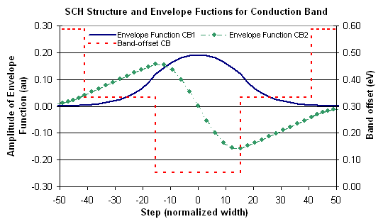
Fig. 3.3.1 Conduction band envelope functions for energy levels 1 and 2.
Similarly, for the Heavy Hole and Light Hole Bands, the energy eigenvalues are calculated and depicted on the screen by the program, and the output file, energy.dat, will be generated for the energy eigenvalues for each band.
The content of this file for the example in section 3.3.4 is as follows:
HEAVY HOLE ENERGY===> -0.223219288877E+00 ERROR= .2395481E-14
HEAVY HOLE ENERGY===> -0.185080559932E+00 ERROR= .3141766E-14
HEAVY HOLE ENERGY===> -0.175552677060E+00 ERROR= .2217630E-14
HEAVY HOLE ENERGY===> -0.118303564930E+00 ERROR= .3822063E-14
HEAVY HOLE ENERGY===> -0.232927951139E-01 ERROR= .2486083E-14
HEAVY HOLE ENERGY===> 0.400110417946E-01 ERROR= .2083172E-14
The first energy eigenvalue for the above calculation corresponds to the last line; the second energy eigenvalue corresponds to the second from bottom and so on. This is because the energy values are negative quantities for Heavy/Light Hole Band case (below the zero reference as shown in Fig. 3.1.1); therefore, the smaller negative energy value corresponds to the higher energy eigenvalue in the valence band energy levels.
If the Schrödinger wave function for the energy eigenvalues is asked to be calculated, then an output file, whose name is to be provided by the user, will be generated. This file contains the band-offset for valence band Heavy/Light Hole and the envelope function for the given energy eigenvalues. For field envelope calculations of each eigenvalue, a separate output file is generated and it should be named by the user. For this example, they are named as hh1.dat, hh2.dat and so on for the Heavy Hole Band; lh1.dat, lh2.dat and so on for the Light Hole Band. The content of these files are similar to the files for the conduction band.
Figure 3.3.2 is the plot for the heavy hole valence band envelope functions for energy levels 1, 2, and 3. This is the combination of files hh1.dat, hh2.dat, and hh3.dat in this example.
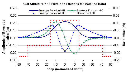
Fig. 3.3.2 Heavy hole valence band envelope functions for energy levels 1, 2, and 3.
The plots for the Light Hole Band envelope functions are similar to the plots for the Heavy Hole Band envelope functions, which are shown in Fig. 3.3.2.
In this Section, the energy eigenvalues will be calculated for conduction band, heavy hole band, and light hole band. The material system InGaAlAs/InGaAlAs was chosen as the example. In Chapter 2, the band offset and the material composition were calculated and the results were written to files cbandeg.dat and vbandeg.dat as an output. The detailed discussion of these files can be found in section 2.2, and for energy calculations these files are used as input files. The band offset diagrams for conduction and valence bands are shown in Fig. 3.4.1.
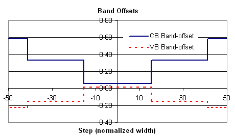
Fig. 3.4.1 Conduction Band and Valence Band offset diagram for the example.
In the following sections, 3.4.1 and 3.4.2, the software will be run continuously for the example material system for the same set of parameters chosen in section 2.3. The explanations for running the software for this example can be found in section 3.2. The explanations of input and output files for this section are in section 3.3.
The program is launched in the program folder. It provides the information about the steps in the program.
C:\Gain>qwl
************************************************************************
THE MAIN PROGRAM IS ONLY A
CALLING PROGRAM, WHICH
CONTAINS THREE MAJOR PARTS
(MORE THAN 20 SUBROUTINES)
FIRST SELECT MATERIAL
PARAMETER,.
SECOND SELECT ENERGY LEVELS IN
BOTH BANDS,
THIRD FIND THE G(J), G(WAVELENGTH)
AND RATE EQUATIONS.
***********************************************************************
A. MAKING
THE SELECTION TO CALCULATE THE ENERGY VALUES
This step asks for layer parameters and produces the outputs for energy eigenvalues. It also writes these values into an output file called energy.dat.
MAKE YOUR SELECTION NOW!
ENTER 1 FOR THE NECESSARY PARAMETERS
2
FOR THE ENERGY VALUES OF CONDUCTION BAND
3 FOR THE ENERGY VALUES OF
HEAVY HOLE BAND
4 FOR THE ENERGY VALUES OF
LIGHT HOLE BAND
5 FOR THE LASER G-J AND
G(LAMBDA)
6 FOR RATE EQUATIONS (TWO
SECTION MODEL INCLUDED)
7 FOR EXIT
> 2
q
Note: This selects the calculation of energy
values for conduction band.
B. INPUTTING THE STRUCTURE PARAMETERS
The input parameters will be provided here. The explanations for the parameters are found in section 3.2.2.
INPUT THE NUMBER OF QUANTUM WELLS NUM=?
> 1
q Note: There is a single quantum well for this example.
INPUT TOTAL LAYERS FOR STRUCTURE--N ODD
INPUT N=
> 5
q Note: Total number of layers is 5 for this structure. See Fig. 3.4.1.
INPUT THE LOWEST POTENTIAL LAYER(1st Q-WELL) IC= ?
> 3
q
Note: The lowest potential layer for CB is the
quantum well layer. Here the first quantum well layer is used as the input, which
is layer 3.
INPUT THE SELECTED CENTER LAYER OF STRUCTURE ICR=
> 3
q Note: This is a five-layer structure. See Fig. 3.4.1.
C. SELECTING THE MATERIAL SYSTEM
The material system will be
selected.
************************************************************************
INPUT I=1 FOR AlGaAs
I=2 FOR InGaAsP
I=3 FOR In1-xGaxAs/InGaAsP/InP
I=4 FOR InGaAlAs/InGaAlAs
I=5 FOR GaInP/(AlGa)0.5In0.5P/AlInP
I=6 FOR InGaAs/AlGaAs/AlGaAs
I=7 FOR InGaAs/InGaAsP/Ga0.51In0.49P(GaAs)
I=8 FOR AlyInxGa1-x-yAs/AlzGa1-zAs/GaAs
I=9 FOR InzGa1-zAs/AlxGayIn1-x-yAs/InP
I=10 FOR
InGaAlAs/InGaAlAs/AlAsxSb1-x(InP)
I=11 FOR
InzGa1-zAs/AlxGayIn1-x-yAs/AlAsxSb1-x
I=12 FOR
In(y)Ga(1-y)As(x)N(1-x)/GaAs
I=13 FOR
InGaAs/In(1-y)Ga(x)As(y)P(1-y)/GaAs
INPUT I= ?
************************************************************************
> 4
q Note: For this example material system 4 was chosen.
D. CALCULATION OF ENERGY VALUES
The energy eigenvalues are calculated and displayed on the screen. Also, they are written to an output file called energy.dat.
ENERGY EIGENVALUE ===>
0.480716488922E-01 ERROR= .2389607E-14
ENERGY EIGENVALUE ===> 0.292753578324E+00
ERROR= .3164269E-14
ENERGY EIGENVALUE ===>
0.432969897088E+00 ERROR= .1487524E-14
E. CALCULATION OF ENVELOPE FUNCTIONS AND CONFINEMENT
FACTORS
This calculates the envelope functions if asked. It writes the outputs to data files whish will be named by the used.
FOR CHECKING THE Schrodinger WAVE FUNCTION INPUT I==> 1
SKIP INPUT I ==> 2
I=?
> 1
q Note:
In order to calculate the envelope functions selection 1 is chosen. If 2 is selected
it will skip envelope calculations.
INPUT THE EIGENVALUE
EIGEN VALUE=
> 0.480716488922E-01
q
Note: This is the eigenvalue for the first
energy level in CB. Any of these values can be selected to calculate the
corresponding envelope functions.
> cb1.dat
q
Note: The program writes the calculation results
of envelope function into this file. The user can name the file arbitrarily.
The confinement factors for each layer corresponding to the selected eigenvalue envelope function are calculated and displayed on the screen.
CONFINEMENT FACTOR OF 1 th
LAYER = 0.17059025E-04
CONFINEMENT FACTOR OF 2 th
LAYER = 0.46544414E-01
CONFINEMENT FACTOR OF 3 th
LAYER = 0.90687705E+00
CONFINEMENT FACTOR OF 4 th
LAYER = 0.46544414E-01
CONFINEMENT FACTOR OF 5 th
LAYER = 0.17059025E-04
F. MORE CALCULATION FOR THE ENVELOPE FUNCTIONS AND
CONFINEMENT FACTORS
In order to continue calculating the envelope functions for the energy eigenvalues of interest, Step E in this Section is repeated for each eigenvalue of interest. As an example the envelope function for second energy level is calculated below.
INPUT NEW EIGENVALUE--> 1, BACK TO MAIN PAGE--> 2
SELECT=?
> 1
q Note: To calculate the envelope function for another energy level selection 1 is chosen.
INPUT THE EIGENVALUE
EIGEN VALUE=
> 0.292753578324E+00
q
Note: The energy eigenvalue of interest is
provided. In this example, the value for 2nd energy level is chosen.
INPUT THE NAME OF OUTPUT FILE
>
cb2.dat
q
Note: This is the file that software will write
calculation results. The user can choose any name.
The confinement factors for each layer corresponding to the selected eigenvalue envelope function are calculated and displayed on the screen.
CONFINEMENT FACTOR OF 1 th
LAYER = 0.20929892E-02
CONFINEMENT FACTOR OF 2 th
LAYER = 0.22590594E+00
CONFINEMENT FACTOR OF 3 th
LAYER = 0.54400214E+00
CONFINEMENT FACTOR OF 4 th
LAYER = 0.22590594E+00
CONFINEMENT FACTOR OF 5 th LAYER = 0.20929892E-02
INPUT NEW EIGENVALUE--> 1, BACK TO MAIN PAGE--> 2
SELECT=?
> 2
q
Note: If Back
to Main Page (selection 2) is selected the energy calculation will be
terminated.
ENTER 1 FOR
THE NECESSARY PARAMETERS
2
FOR THE ENERGY VALUES OF CONDUCTION BAND
3 FOR THE ENERGY VALUES OF
HEAVY HOLE BAND
4 FOR THE ENERGY VALUES OF
LIGHT HOLE BAND
5 FOR THE LASER G-J AND
G(LAMBDA)
6 FOR RATE EQUATIONS (TWO
SECTION MODEL INCLUDED)
7 FOR EXIT
> 7
q
Note: This selection will terminate the program.
BACK TO FIRST SELECTION PAGE !
C:\Gain>
The Steps A, B, and C are similar to conduction band calculations in section 3.4.1.
After Step C, the strain values should be provided for both heavy hole and light hole band energy calculations.
A. STRAIN INPUT
*******************************************************
DOES THE STRUCTURE STRAIN OR STRAIN-COMPENSATED?
IF STRAIN ONLY INPUT 1, STRAIN-COMPENSATED INPUT 2
INPUT SELECT = ?
> 2
q
Note: The structure in this example is strain
compensated, so 2 is selected.
INPUT BARRIER STRAIN =?
> 0.008776922
q Note: This value is the strain parameter from 2.1
After providing the strain input for this step, the rest of the steps for heave hole and light hole energy calculations (Steps D, E, and F) are similar to conduction band energy calculations as in section 3.4.1.
In the previous chapters, computations of material compositions, band offsets, and energy levels are discussed. After these computations, the properties of the designed semiconductor laser are simulated using the GAIN program including the simulations of the gain spectrum, threshold current density, and slope efficiency.
The basic theories
involved in the simulations are discussed in A.2.4.1,
and the explanations of input and output files are provided in Sections 4.2 and
4.3 of this chapter. Finally, an
example of how to run the GAIN program for gain and laser characteristics
simulations is given in section 4.4.
The simulations of the optical gain in the active region of the lasers are complicated. The GAIN program utilizes the accurate model of the optical gain with anisotropic factor, overlap factor and Lorentz lineshape included, as shown in Equation 4.1 [3]:
 (
(A4.2.1)
where MB … The momentum matrix element
E … The optical energy
… Vacuum permittivity
N … Refractive index
W … Width of the well
C … The speed of light
mr,ij … The reduced effective mass
Cij … The overlap factor
Aij … The anisotropic factor
fc, fv … The Fermi-Dirac distribution of the conduction and valence bands.
H … The step function
L(E) … The Lorentz lineshape
In the equation 4.1, the Fermi-Dirac
distributions of the conduction and valence bands ![]() need to be computed.
So it is necessary to calculate the quasi-fermi levels
need to be computed.
So it is necessary to calculate the quasi-fermi levels![]() using equation 4.2 for conduction band and equation 4.3 for
valence band [4].
using equation 4.2 for conduction band and equation 4.3 for
valence band [4].
![]() , (4.2)
, (4.2)
![]() (4.3)
(4.3)
where N is the carrier concentration of the electrons in the conduction band,
P is the carrier concentration of the holes in the valence band,
![]() are quasi-fermi
levels,
are quasi-fermi
levels,
m*n and m*lh,hh are the in-plane effective masses of the electrons and holes,
Lz is the quantum well width,
k is the Boltzmann constant, and
![]() is the reduced plank
constant.
is the reduced plank
constant.
In the above equations 4.2 and 4.3, the quasi-fermi
levels ![]() can be solved with a
given carrier concentration, and known energy levels which have been
calculated in the previous steps of
GAIN program.
can be solved with a
given carrier concentration, and known energy levels which have been
calculated in the previous steps of
GAIN program.
In summary, from the above equations, the Optical/Mode Gain as a function of wavelength and Optical/Mode Gain as a function of photon energy are computed. The example of how to run the GAIN program to get the results is shown section 4.3 of this Chapter.
The GAIN program provides two threshold current densities (Jth) of the designed laser that correspond to two different methods. The first method is to match the threshold condition [5], and the second method is to use McIlroy theory [5]. This subsection gives the brief introduction of the two methods.
1. Threshold condition method.
In order for the laser to lase, the mode gain which is the product of the optical gain and confinement factor has to overcome the total loss which is the sum of the material loss and mirror loss, as shown in Equation 4.4. The GAIN program finds the current density at which the mode gain overcomes the loss to be the threshold current density of the laser structure [5].
In this method, the GAIN program first simulates the threshold current density for a single quantum well structure, and then use the product of the number of quantum wells and the threshold current density of the single quantum well to approximate the threshold current density of the multiple quantum well, as shown in equation 4.5.
![]() (4.4)
(4.4)
Jth-MQW = n * Jth-SQW (4.5)
where n: number of quantum wells,
ai: intrinsic loss,
L: cavity length,
R1, R2: reflectivities of the facets.
2. McIlroy method.
For the McIlroy method, the threshold current density is approximated by the empirical equation 4.6 [5]:
![]() (4.6)
(4.6)
where Jo is obtained in Figure 4.1.1, and the optimum number of quantum wells (Nopt) is calculated by equation 4.7 [5]:
 (4.7)
(4.7)
where Go is acquired in Figure 4.1.1,
Gsqw is the confinement factor of a single quantum well,
ai: intrinsic loss,
L: cavity length,
R1, R2: reflectivities of the facets.
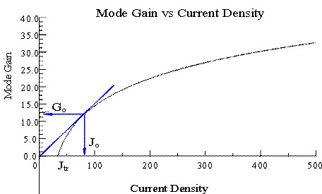
Fig. 4.1.1. Mode gain as a function of current density for a single QW structure.
The optical output power of the laser as a function of injected current and the slope efficiency is simulated in GAIN program [6] using the equation 4.8.
 (4.8)
(4.8)
where P: the output power of the laser
ai: intrinsic loss
am: mirror loss
hi: internal quantum efficiency
W: width of the quantum well
L: length of the quantum well
n: photon frequency
Jth: threshold current density
q: elementary charge
h: plank constant
R1, R2: reflectivities of the facets.
The slope efficiency can be calculated from the L-I curve DP/DI, as shown in Figure 4.1.2.

![]()
![]()
![]()
![]()
![]()
![]()
![]()
![]()
![]()
![]()


Figure 4.1.2 L-I curve of the laser
The input file is
needed at the beginning of the step 5 of the gain program. It includes the
basic input data for the laser structure such as the compositions, width of
well, effective index, lasing wavelength, the energy levels etc. In the
following, the input file is broken into 6 parts to give detail explanation.
Note: Here we use the material system No. 4 ( AlGaInAs/InP ) as an
example.
Part 1:
cccccccccccccccccccccccccccccccccccccccccccccccccccccccccccccccccccccccc
c 1. Input the
compositions, width of well, effective index c
c and lasing
wavelength.
c
c Ex:
xx,xz,qy,xy,lx,n,lam c
c for different
materials the following are the forms of inputs. c
c
c
c w -- > well,
b -- > barrier cxz and cxy for
cladding. c
c
c
c a. AlxGa1-xAs : xx (Al w) xz (Al b) qy (0) xy
(0) c
c b. In1-xGaxAsyP1-y : xx (Ga w) xz (Ga b) qy (As
w) xy (As b) c
c c. In1-xGaxAs/InGaAsP : xx (Ga w) xz (Ga b) qy
(0) xy (As b) c
c d. AlxGayIn1-x-yAs/InP : xx (Ga w) xz (Ga b) qy
(Al w) xy (Al b)c
c e.
c
c f. InxGa1-xAs/AlGaAs : xx (In w) xz (0) qy (0)
xy (Al b) c
c g.
c
c h. AlyInxGa1-x-yAs/AlGaAs : xx (Al w) xz (al b)
qy (In w) xz (0)c
c i. In1-xGaxAs/AlGaInAs : xx (In w) xz (0) qy (Al
b) xy (Ga b) c
c j. In(y)Ga(1-y)As(x)N(1-x) :xx(As w),xz(As,
b),qy(In w),xy(In b)c
c k. InGaAs/InGaAsP/GaAs: xx (In w), (0), xz(Ga w)
xy (As b)
cccccccccccccccccccccccccccccccccccccccccccccccccccccccccccccccccccccccc
0.21964924 0.34879557
0.0801355 0.2505339 6.0
3.218741 1.5
NOTE for Part 1 of the Input
File:
(a):Here we use the material system AlGaInAs/InP as an example.
(b):The first 4 numbers come from the file cbandeg.dat or vbandeg.dat, which are the output files of step 1 ( explained in chapter 2 ). The order is: quantum well x composition, barrier x composition, quantum well y composition, barrier y composition. Ps: Please refer to the Appendix for the definition of x and y which are different for different material systems.
(c): The width of well should be chosen in a reasonable ra
nge, the effective index can be got by using the WAVEGUIDE or MODEIG software or refer to some book to calculate.
(d): The units of the width of quantum well and the lasing wavelength are nm and um.
Part 2:
cccccccccccccccccccccccccccccccccccccccccccccccccccccccccccccccccccccccc
c 2. Input the
energy gap,temperature, barrier band edges(both bands)
c Ex:
eg,temp,ec,ev
c
cccccccccccccccccccccccccccccccccccccccccccccccccccccccccccccccccccccccc
0.683804 298 0.3327401 0.1241536
NOTE for Part 2 of the Input
File:
(a): Energy gap here refer to the QW Eg, which is equal to 1.24/quantum well wavelength (um), this is calculated in the step 1 of the gain program.
(b): Enter the temperature, please note that the material loss, optical Auger coefficient, and other parameters need to be adjusted for different temperature.
(c): Find the barrier band edges
for both conduction and valence bands from the output files of the step 1:
cbandeg.dat and vbandeg.dat. The barrier band edge of the valence band should change to the opposite sign value
of the real number.
Part 3:
cccccccccccccccccccccccccccccccccccccccccccccccccccccccccccccccccccccccc
c 3. Input the
ist level sub-band energy levels. c
c Ex:
ec1,eh1,el1
c
cccccccccccccccccccccccccccccccccccccccccccccccccccccccccccccccccccccccc
0.132273291719
0.584032029186E-02
0.978425521147E-01 1 1 1
NOTE for Part 3 of the Input File:
(a): The order of the input data is: the first energy levels of conduction, heavy hole, light hole and the second energy levels of conduction, heavy hole, light hole. These data come from the step 2, 3 and 4 of the gain program, which are calculated from the step 2, 3, and 4, and can be found in the output file: energy.dat.
(b): The values from the heavy hole and light hole should change to the opposite sign value of the real number.
(c): If the second energy levels of conduction are above the barrier band edge, use 1 to replace the value of ec2; if the second energy levels of valence band are under the barrier band edge, use 1 to replace the value of eh2 or el2.
Part 4:
cccccccccccccccccccccccccccccccccccccccccccccccccccccccccccccccccccccccc
c 4. Input the
material loss, reflectivities, number of quantum c
c wells and
beta(for spontaneous emission). c
c Ex:
alpha,r1,r2,mm,beta. c
cccccccccccccccccccccccccccccccccccccccccccccccccccccccccccccccccccccccc
12.0d0 0.30 0.30 1 5.D-5
NOTE for Part 4 of the Input File:
These values are good for starting.
(1): The loss and reflectivity (r1, r2) are key factors to determine the threshold condition.
(2): If the number of quantum wells (mm) is more than one, then the output files
*.gjr and *.gja will calculate
the G-J file for multiple wells which is not necessary.
(3): The beta is only used in dynamic calculation and this number here is an advised parameter for ridge and BH laser simulations.
Part 5:
cccccccccccccccccccccccccccccccccccccccccccccccccccccccccccccccccccccccc
c 5. Input the
cavity length, ridge width, internal efficiency c
c Auger,
strain(except AlGaAs,put 0) and confinement factor. c
c Ex:
cl,cw,etha,ca,es,confine c
cccccccccccccccccccccccccccccccccccccccccccccccccccccccccccccccccccccccc
750.D-4 3D-4 0.96
1.00d-29 0.000 0.009834488
NOTE for Part 5 of the Input File:
(a): The cavity (cl) and width (cw) of ridge are structure features, the units of cavity length and ridge width are cm.
(b): The internal efficiency (etha) and Auger (ca) can refer to papers for the latest values.
(c): The strain (es) is just ignored for all material systems except for GaAs/AlGaAs)
(d): Give the initial guess of the confinement factor of the quantum well.
Part 6:
cccccccccccccccccccccccccccccccccccccccccccccccccccccccccccccccccccccccc
c 6. Input the
cladding composition and band edges.
c
c Ex:
cxz,cxy,ecc,evv c
cccccccccccccccccccccccccccccccccccccccccccccccccccccccccccccccccccccccc
0.48 0.0
0.5859193 0.2278575
NOTE for Part 6 of the Input File:
Find the cladding composition (cxz and cxy) and the band edges (ecc and evv) from the cbandeg.dat or vbandeg.dat, the band edges from the vbandeg.dat should change to the opposite sign value of the real number.
There are total 17 output files containing important laser information from the step 5 of the gain program. Table 4.1 shows details, and the plots of the output files are also provided in 4.3.2.
Table 4.3.1 : The table for the output files.
|
File name |
Content |
X axis |
Y axis |
|
Cfermil |
Quasi
Fermi-level for conduction band |
Number of
N-carrier (/cm3) |
C band Quasi
Fermi Level (eV) |
|
Vfermil |
Quasi
Fermi-level for valence band |
Number of
P-carrier (/cm3) |
V band Quasi
Fermi-Level (eV) |
|
****.ant |
Anti-guiding factor as function of current density |
Current Density (A/cm2) |
Anti-guiding Factor |
|
****.cp |
Gain compression |
carrier density (*E18) |
Gain compression (cm3) |
|
****.dg |
Differential gain |
Carrier density (*E18) |
Differential Gain (cm2) |
|
****.gc |
Peak material gain as function of carrier density |
Carrier
density (*E18) |
Peak Material Gain (1/cm) |
|
****.gja |
Peak material gain as function of threshold current density |
Current Density (A/cm2) |
Peak Material Gain (1/cm) |
|
****.gjr |
Peak mode gain
as function of current density |
Current Density (A/cm2) |
Peak Mode Gain
(1/cm) |
|
****.lek |
Leakage current as function of carrier concentration |
Leakage Current (A/cm2) |
Carrier Concentration (1/cm3) |
|
****.ric |
Carrier induced refractive index change |
Number of Carrier |
Refractive Index Change |
|
****.pi |
P-I relation: use single well times # of wells. |
Power (mW) |
Current (mA) |
|
****.pi2 |
P-I relation: use McIlory method for single well,Then with Nopt |
Power (mW) |
Current (mA) |
|
****.rq |
Relaxation oscillation frequency as function of J (above Jth) |
Current Density (A/cm2) |
Relaxation Oscillation Frequency (Hz) |
|
COGL.txt |
Convolution optical gain (lambda) |
Lasing Wavelength (μm) |
Material Gain (1/cm) |
|
CMGL.txt |
Convolution mode gain (lambda) |
Lasing Wavelength (μm) |
Mode Gain (1/cm) |
|
COGE.txt |
Convolution optical gain (E) |
Photon Energy (eV) |
Material Gain (1/cm) |
|
CMGE.txt |
Convolution mode gain (E) |
Photon Energy (eV) |
Mode Gain (1/cm) |
NOTE: The four names and extensions of txt files: COGL.txt, CMGL.txt, COGE.txt and CMGE.txtare entered by the users.
There are 17 figures according to the 17 output data files that generated from the step 5 of the Gain program as following:

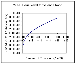
Fig
4.3.2.1: cfermil Fig 4.3.2.2: vfermil
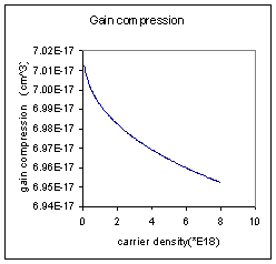
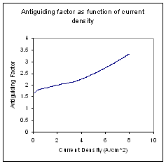
Fig 4.3.2.3: ****.ant Fig 4.3.2.4: ****.cp
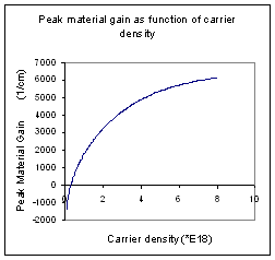
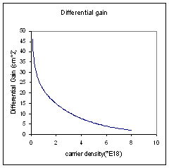
Fig 4.3.2.5: ****.dg Fig 4.3.2.6: ****.gc
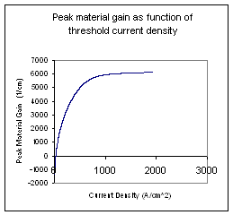
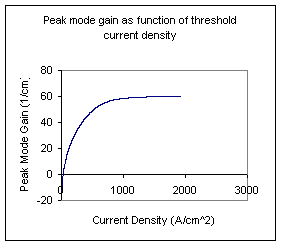
Fig 4.3.2.7:
****.gja
Fig 4.3.2.8: ****.gjr
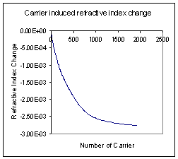
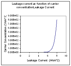
Fig 4.3.2.9:
****.lek Fig 4.3.2.10: ****.ric
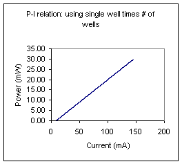
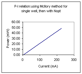
Fig 4.3.2.11: ****.pi Fig 4.3.2.12: ****.pi2
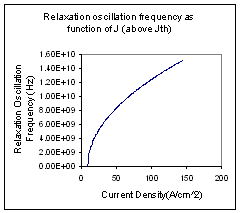
Fig 4.3.2.13: ****.rq
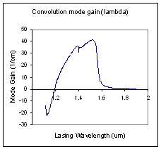
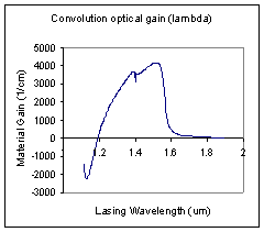
Fig 4.3.2.14: COGL.txt Fig 4.3.2.15: CMGL.txt
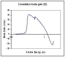
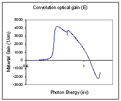
Fig 4.3.2.16:
COGE.txt
Fig
4.3.2.17: CMGE.txt
In this section, an example will be shown to explicate the steps of running the 5th part of the Gain program “FOR THE LASER G-J AND G (LAMBDA)”. To run this part, the previous 4 parts must be followed in order to get the required parameters and input files. Detailed steps are shown below:
THE INPUT FILE NAME=
> in1.tex-----------------------or any other name of a txt file.
Ø Note: The file “in1.tex” is built based on the output from previous 4 parts. The detailed description about the contents of the input file and how to build them are already given in section 4.2 “input file”.
SELECT MATERIAL=?
1--AlGaAs
2--InGaAsP
3--In1-zGazAs/InGaAsP/InP
4-- InGaAlAs
5--GaInP/AlzGawIn1-z-wP/Al0.5In0.5P
6-- InxGa1-xAs/AlxGa1-xAs/AlGaAs
7--In1-xGaxAs/InGaAsP/GaxIn1-xP(X=0.51) MATCHED TO GaAs
8--AlyInxGa1-x-yAs/AlzGa1-zAs/GaAs
9--InzGa1-zAs/AlxGayIn1-x-yAs/InP
10-- InGaAlAs/InGaAlAs/AlAsSb
11--InzGa1-zAs/AlxGayIn1-x-yAs/AlAsSb
12--In(y)Ga(1-y)As(x)N(1-x)/GaAs
13--InGaAs/In(1-x)Ga(x)As(y)P(1-y)/GaAs
INPUT SELECTION
> 4-----------------------or any other material type
Ø Note: In order to keep the consistency, the material selected here is the same as the material system used in the examples given in previous chapters.
INPUT MODE = ? FOR TE--> MODE =1, FOR TM--> MODE =2
INPUT TE OR TM ?
> 1
Ø Note: TE and TM are two kinds of electromagnetic field modes. TE refers to transverse-electric, and TM means transverse-magnetic.
IF EL1 BELOW EH1 THEN SELECT 1, OTHERWISE SELECT 2
SELECTION=?
> 1
Ø Note: EL1 refers to the energy of 1st light hole valence band. EH1 refers to the energy of 1st heavy hole valence band. From the file “energy.dat” generated from previous parts 3-4, we can find EL1 = -0.897913179665E-01, and EH1 = -0.153962179517E-02. Since EL1 < EH1, we select 1.
************************************************************************ CALCULATE THE EFFECTIVE MASS ************************************************************************
FOR QUASI-FERMI LEVEL SELECT=1,
FOR READ EXISTING QUASI-FERMI LEVEL SELECT=2
SELECT=?
> 1
Ø Note: In most cases, “1” is selected. If a file of quasi-fermi level is already existed and there is no any change to those parameters of the laser structure, “2” can be selected to save the calculation time.
After that, quasi-fermi level is calculated and two output files “cfermil.dat” and “vfermil.dat” are generated. In addition, another eight files named “in1.tex.ant”, “in1.tex.cp”, “in1.tex.dg”, “in1.tex.gc”, “in1.tex.gja”, “in1.tex.gjr”, “in1.tex.lek” and “in1.tex.ric” are generated too. Then, values for G(J), G(N), Jtr, Ntr and the optimum number of quantum well are shown up. The meaning and usage of those files are explained in section 4.1 “Theories for computation of Gain and Laser properties” and section 4.3 “output files”.
************************************************************************
J(LEAKAGE)=0.811020D-02 A/cm^2 N=0.239674D+19 1/cm^3
J(LEAKAGE)=0.845424D-02 A/cm^2 N=0.241654D+19 1/cm^3
……
……
……
J(LEAKAGE)=0.784174D+03 A/cm^2 N=0.798020D+19 1/cm^3
J(LEAKAGE)=0.812685D+03 A/cm^2 N=0.800000D+19 1/cm^3
************************************************************************
G(J) PARAMETERS FROM SINGLE WELL
Go=0.158181D+02 1/cm Jo=0.954942D+02 A/cm^2
G(N) PARAMETERS FROM SINGLE WELL
NGo=0.160843D+04 1/cm XNo=0.911779D+18 1/cm^3
Jtr=0.351304D+02 A/cm^2 NTR=0.335425D+18 1/cm^3
THE OPTIMUM NUMBER OF QUANTUM WELL FOLLOWS THE ARTICLE
BY McIlory et al. IEEE JQE-21 1985.
THE OPTIMUM NUMBER OF QUANTUM WELL Nopt = 2
INPUT Nopt(CAN BE DIFFERENT FROM ABOVE CALCULATION)=?
> 1
Ø Note: This is the optimum number of quantum well.
NUMBER OF QUANTUM WELL (MAY OR MAY NOT BE Nopt)=?
> 1
Ø Note: This is the number of quantum well designed by the users.
Ø Here, files named “in1.tex.pi”, “in1.tex.pi2”, and “in1.tex.rq” are generated in the same directory. After that, threshold current density “Jth”, threshold current “Ith” and the slope efficiency “B” are calculated out. Detailed explanation for threshold current density, threshold current and the slope efficiency can be found in section 4.1.2.
The output are shown below.
************************************************************************
1ST CHECK USE SINGLE WELL TIMES # OF WELLS
************************************************************************
2ND CHECK FOLLOWS FORMULA BY McIlory IN IEEE
JOURNAL OF QUANTUM ELECTRONIC QE-21 1985.
**************************************************
Gth= 28.0530 1/cm Nth=0.170376D+19 1/cm^3 IY= 82
1ST CHECK Jth= 190.71442056 A/cm^2
2ND CHECK Jth= 99.47316 A/cm^2
1ST CHECK Ith=0.429107D+01 mA NUMBER OF WELLS= 1
2ND CHECK Ith=0.223815D+01 mA
************************************************************************CALCULATE THE P-I RELATION
NDATA= 319
************************************************************************
CALCULATE THE SLOPE: mW/mA Y=A+BX
CONSTANT A= -0.9372099 SLOPE B= 0.2184091
Ø Note: 1st method checks the threshold condition and the G-J curves and then decides the Jth and others. The 2nd check is strictly following the Maclloy theory. Detailed explanation for these two methods can be found in section 4.1.2.
***********************************************************************
INPUT POWER
INPUT
> 0
Ø Note: Because of the updating of new method, Line width calculation is not recommended here. New version of software is under construction.
INPUT 1 FOR THE DYNAMIC CALCULATION. 2 FOR SKIP
INPUT =
> 2
Ø Note: New version of dynamic calculation is under construction.
K-FACTOR= 0.33294 nS MAXIUM FREQ.= 26.6891 GHz
************************************************************************
INPUT 1 FOR CALCULATE THE GAIN(E) RELATION.
INPUT 2 FOR CALCULATE THE LINEWIDTH ENHENCEMENT
FACTOR AND PHOTON ENERGY RELATION
INPUT 3 FOR EXIT THE PROGRAM
THE INPUT # IS
> 1
Ø Note: The calculation of line width enhancement factor and photon energy relation is not recommended here. New version of software is under construction.
INPUT FERMILEVELS IN C-BAND, V-BAND, AND CARRIER DENSITY
> 0.238566456069E+00, 0.666558305734E-02, 2E+18
Ø Note: These values come from the two output files “cfermil.dat” and “vfermil.dat” generated in the previous steps. Based on the different carrier density, the corresponding C-band and V-band fermi-level values can be found in those two files.
CALCULATE THE CONVOLUTION GAIN (E) COEFFICIENT
************************************************************************
INPUT THE NAME FOR THE CONVOLUTION OPTICAL GAIN(LAMBDA)
> opticalgain
Ø Note: Input any name you like for the file of optical gain.
************************************************************************
INPUT THE NAME FOR THE CONVOLUTION MODE GAIN(LAMBDA)
> modegain
Ø Note: Input any name you like for the file of mode gain.
INPUT THE NAME FOR THE CONVOLUTION OPTICAL GAIN(E)
> opticalgaine
Ø Note: Input any name you like for the file of optical gain (E).
************************************************************************
INPUT THE NAME FOR THE CONVOLUTION MODE GAIN(E)
> modegaine
Ø Note: Input any name you like for the file of mode gain (E).
************************************************************************
INPUT 1 FOR REPEAT THE G(E) CALCULATION
INPUT 2 FOR REPEAT THE ALPHA(E) CALCULATION
INPUT 3 FOR EXIT
> 3
Ø
Notes: New version of the alpha (E)
calculation is under construction.
[1] Sandra R. Selmic et al., “Design and Characterization of 1.3-um AlGaInAs-InP Multiple-Quantum-Well Lasers”, IEEE Journal on Selected Topics in Quantum Electronics, vol.7, no. 2, pp340-349, March 2001
[2] Shun Lien Chung, “Physics of Optoelectronic Devices”, John Wiley & Sons, Inc., 1995.
[3] Stephen R. Chinn, Peter S. Zory, and Axel R. Reisinger, “A Model for GRIN-SCH-SQW Diode Lasers”, IEEE J. Quantum Electronics, vol. 24, no. 11, 1988.
[4] Tso-Min Chou, “Theory and Design Application of Strained
Separate-Confinement Heterostructure Quantum Well Lasers”, SMU,
[5] P. W. A. McIlroy, A. Kurobe, and Y. Uematsu, “Analysis and application of theoretical gain curves to the design of multi-quantum-well lasers”, IEEE J. Quantum Electron., QE-21, 1958-1963, 1985.
[6] N. K. Dutta, G.
P. Agrawal, “Semiconductor Lasers”, 2nd
Edition, Van
[7]
Chao-Suan Yeh, Theoretical and
Experimental Investigation of Slab Waveguides with Periodic Grating Layer.
[8] Peter S. Zory, Quantum Well Lasers, Academic Press Inc. 1993
[9] L.A.Coldren, Diode Lasers and Photonic Integrated Circuits, John Wiley & Sons, Inc, 1993
[10]
Myron B. Allen III, Eli L. Isaacson, Numerical analysis for applied science,
[11] Daniel D. McCracken and William S. Dorn, Numerical methods and FORTRAN programming, with applications in engineering and science, New York, Wiley, 1964
This section provides the information of every material system used in GAIN software on:
1.
Materials
used for QW, barrier, cladding and substrate.
2.
The
equations used for calculating the material compositions of quantum well (QW),
barrier and cladding layers. In these equations, the energy gap corresponds to
that of bulk materials. The designer should adjust the energy gap and layer
thicknesses to get the required lasing wavelengths. Usually this process will
be repeated several times for a satisfying design.
3.
Numerical
methods used in calculating the material compositions. The detailed information
on the numerical methods is beyond this manual. Please reference to book [10],
[11] for more information on the numerical methods.
4.
Practical
lasing wavelengths for each material system. Usually a specific material system
can cover a specific range of lasing wavelength. However, in this manual we
give the practically widely used lasing wavelengths for some material systems.
The user can design the semiconductor laser device with reference to the
practical lasing wavelengths for each material system.
If not explicitly tell, the units of wavelength, energy gap, layers width, and lattice constant for all the material systems are mm, eV, Å, Å, respectively.
Table A.1 gives the composition of different parts of the quantum well laser structure
Table A.1 The composition of materials in quantum well, barrier, cladding and substrate.
|
Materia System |
Quantum Well |
Barrier |
Cladding |
Substrate |
|
1 |
AlGaAs |
AlGaAs |
AlGaAs |
GaAs |
|
2 |
InGaAsP |
InGaAsP |
InGaAsP |
InP |
|
3 |
InGaAs |
InGaAsP |
InP |
InP |
|
4 |
InGaAlAs |
InGaAlAs |
InGaAlAs |
InP |
|
5 |
GaInP |
(AlGa)0.5In0.5P |
AlInP |
GaAs |
|
6 |
InGaAs |
AlGaAs |
AlGaAs |
GaAs |
|
7 |
Be substituted by13 |
|||
|
8 |
AlInGaAs |
AlGaAs |
GaAs |
GaAs |
|
9 |
InGaAs |
AlGaInAs |
AlGaInAs |
InP |
|
10 |
InGaAlAs |
InGaAsAs |
AlAsSb |
InP |
|
11 |
InGaAs |
AlGaInAs |
AlAsSb |
InP |
|
12 |
InGaAsN |
GaAs(dilute N) |
GaAs (dilute N) |
GaAs |
|
13 |
InGaAsP |
InGaAsP |
GaAs |
GaAs |
Form of composition: AlxGa1-xAs/AlyGa1-yAs
Parameters to be input: Bulk material wavelengths of QW, barrier and cladding, widths of conduction band, valence band and QW.
Lasing wavelength: <870nm
Screen output: Band gap of QW
Equation for calculating x by wavelength:

Method Used: Direct method
Form of composition: In1-xGaxAsyP1-y,
in output read Ga first then As
Parameters to be input: Bulk material wavelengths of QW, barrier and cladding, widths of conduction band, valence band and QW, strains of quantum well and barrier.
Lasing wavelength: 1.2mm -1.7um
Screen output: Strain, band gap of QW
Equation for calculating x and y by wavelength:
![]()
![]() (Å)
(Å)
When lattice-matched to InP
![]()

Method Used: Damped
Form of composition: In1-xGaxAs/ In1-xGaxAsyP1-y
Parameters to be input: Wavelength the correspond to the band gap, widths
Lasing wavelength: 1.2mm -1.7um
Screen output: Strain, band gap of QW
Equation for calculating x and y by wavelength:
For InGaAs:

We are using Hellwege Formula here.
For InGaAsP:
![]()
![]() (Å)
(Å)
When lattice-matched to InP
![]()

Method Used: Damped
Form of composition: AlyGaxIn(1-x-y)As, in output read Ga first then Al
Parameters to be input: Wavelengths, strain (Can be compressive or tensile). If one of the components in active region is zero, the initial guess for wavelength and strain.
Lasing wavelength:1.3um, 1.55um, 1.6um
Screen output: Strain, band gap of QW
Equation for calculating x and y:
![]()
![]()
Where

![]()
In this material system, we have two selections; 1st Eg relation based on the text book by Dr. Chuang and the 2nd one based on industrial experimental formula.
Method Used: Damped
Form of composition: GaxIn1-xP, AlxIn1-xP
Parameters: Wavelengths and widths, short wavelength
Lasing wavelength: red (about 630nm)
Screen output: Band gap of QW, strain in GaInP
Equation to calculate x and strain:
For GaInP:
Not available yet
For AlxIn1-xP

Method Used: Direct method.
Form of composition: In1-xGaxAs/AlyGa1-yAs
Parameters to be input: Wavelengths
Lasing wavelength: 980nm
Screen output: Band gap of QW. Strain for InGaAs/AlGaAs
Equation for calculating x or y:
For InGaAs:

For AlGaAs(x<0.4 ![]() ):
):
![]()
Method Used: Direct method.
7
InGaAs/InGaAsP/Ga0.51In0.49P
(Substrate: GaAs)
This material system is not used any more
and is substituted by material system 13.
Form of composition: AlyInxGa1-x-yAs/AlzGa1-zAs/GaAs
Parameters to be input: Wavelengths, Y and X values
Lasing wavelength: 808nm-980nm
Screen output: Band gap of QW. BANDGAP again, WELL LATTICE, BARRIER
LATTICE, STRAIN
Equations for calculating x, y and z:
For AlInGaAs
![]()
![]()
Where
![]()
For AlGaAs

Please
substitute x by z for AlGaAs. In the future z has the same meaning as x in
material composition formulas.
Method Used: Damped
Form of composition: InzGa1-zAs/AlxGayIn1-x-yAs/InP
Parameters: Wavelengths
Lasing wavelength: 1.3um, 1.55um, 1.6um
Screen output: Band gap of QW
CALCULATE THE In(z)Ga(1-z)As QUANTUM WELL--Z
BARRIER Al(x)Ga(y)In(1-x-y)As AND
CLADDING Al(xc)Ga(yc)In(1-xc-yc)As
X,Y--FOR BARRIER,XC,YC--FOR CLADDING and Z
CHECK STRAIN= 1.289076522918892E-002
Equation for calculating x, y and z:
For InGaAs
![]()
![]()
For AlInGaAs

![]()
Where
![]()
Method Used: Direct method
Form of composition: AlyGaxIn1-x-yAs/ AluGavIn1-u-vAs/AlAszSb1-z
Parameters to be input: Compress or tensile, J=, strain
Lasing wavelength: Long wavelength (>1.3um)
Screen output: Band gap of QW, THE MATCHED BARRIER AND CLADDING COMPOSITION
X,Z--FOR BARRIER,XC,ZC--FOR CLADDING
Equations for calculating x, y/(u, v) and z by wavelength:
For AlInGaAs

![]()
Where
![]()
For AlAsSb
Not available yet.
Here z has the same meaning as x in material composition.
Method Used: Not available yet.
Form of composition: In(z)Ga(1-z)As, Al(x)Ga(y)In(1-x-y)As, AlAs(xc)Sb(1-xc)
Parameters to be input: wavelengths
Lasing wavelength: 1.3um
Screen output: The band gap of QW
X, Y--FOR BARRIER, XC, YC--FOR CLADDING,
STRAIN
Equations for calculating x, y z and xc:
For InGaAs:

We are using Hellwege Formula here.
For AlInGaAs

![]()
Where
![]()
For AlAsSb:
Not
available yet.
Method Used: Not available yet.
Form of composition:
InyGa1-yAsxN1-x
Parameters to be input: wavelengths, strain
Lasing wavelength: 1.3um
Screen output: Band gap of QW, strain vector, strain, AZ2
Equation for calculating x:
For InGaAsN
![]()
![]()
Method Used: Damped
Form of composition:
Quantum well In(1-x)Ga(x)As(y)P(1-y), Barrier
In(1-y)Ga(y)As(x)P(1-x)
Parameters to be input: Wavelengths
Lasing wavelength: 980nm
Screen output: STRAIN FOR InGaAs/InGaAsP/GaAs,
Equation for calculating x and y:
For InGaAsP
![]()
![]() (Å)
(Å)
When lattice-matched to GaAs
![]()
![]()
Method Used: Bauhuber method.
Two examples demonstrate how to generate CBANDEG.DAT and VBANDEG.DAT files using the “GAIN” software. One example is a single-quantum-well laser with GRIN structure, and the other is a multiple-quantum-well laser with GRIN structure.
This example shows how to generate
CBANDEG.DAT and VBANDEG.DAT files for a single-quantum-well laser with GRIN
structure. Five steps, consisting of Select functions, Select materials, Input
the structure parameters, Input strain, and Check output files, are involved in
this procedure. After completing these five steps, we can find CBANDEG.DAT and VBANDEG.DAT
in the current directory. Table B.1.1 summarizes input parameters.
TABLE B.1.1 Input parameters
|
Layers |
l ( (μm)) |
Strain |
Length (Å) |
|
QW (InGaAlAs) |
1.56 |
-0.0117 |
100 |
|
Barrier (InGaAlAs) |
1.3 |
0 |
100 |
|
Cladding (InGaAlAs) |
1.1 |
|
1000 |
Step 1: Select function
ENTER
1 FOR THE NECESSARY PARAMETERS
2 FOR THE ENERGY VALUES OF CONDUCTION
BAND
3 FOR THE ENERGY VALUES OF HEAVY HOLE
BAND
4 FOR THE ENERGY VALUES OF LIGHT HOLE
BAND
5 FOR THE LASER G-J AND G(LAMBDA)
6 FOR RATE EQUATIONS(TWO SECTION MODEL
INCLUDED)
7 FOR EXIT!
1
Note: To input the necessary parameters shown in table I
Step 2: Select material
ENTER
1 FOR AlGaAs/AlGaAs
2 FOR InGaAsP/InGaAs
3 FOR InGaAs/InGaAsP/InP
4 FOR InGaAlAs/InGaAlAs
5 FOR GaInP/(AlGa)0.5In0.5P/AlInP
6 FOR InGaAs/AlGaAs/AlGaAs
7 FOR
InGaAs/InGaAsP/Ga0.51In0.49P(MATCHED GaAs)
8 FOR AlyInxGa1-x-yAs/AlzGa1-zAs/GaAs
9 FOR InzGa1-zAs/AlxGayIn1-x-yAs/InP
10 FOR
InGaAlAs/InGaAlAs/AlAsxSb1-x(matched InP)
11 FOR InzGa1-zAs/AlxGayIn1-x-yAs/AlAsxSb1-x
12 FOR EXIT, BACK TO MAIN PAGE!
4
Note: Select the material system. This example uses InGaAlAs/InGaAlAs , we select number 4
Step 3: Input the structure parameters
INPUT THE LAYER # FOR
GRIN STRUCTURE(STEP)
STEP N=
11
Note: Input the number of the Separate Confinement Heterostructure (SCH) layer. This example uses a 10-step SCH layer in each side of the quantum well, and the input value is 11 (10+1). If the designed laser has no GRIN structure, the input value is 2.
INPUT THE WELL
WAVELENGTH (μm)
1.56
Note: Input the wavelength  , where
 ![]() is the energy bandgap
of the active material. This value must be larger than the desired lasing
wavelength.
is the energy bandgap
of the active material. This value must be larger than the desired lasing
wavelength.
INPUT THE BARRIER
WAVELENGTH (μm)
1.3
Note: Input the barrier wavelength. This value must be smaller than the desired lasing wavelength.
INPUT THE CLADDING
WAVELENGTH (μm)
1.1
Note: Input the cladding wavelength. This value must be smaller than the Barrier wavelength.
INPUT CLADDING,
BARRIER, QUANTUM WELL WIDTH (Å)
1000 100 100
Note: Input the width of the cladding layer, the barrier and the quantum well. Each item is separated by a space. Generally, the width of the quantum well should be smaller than 150 Å.
FOR AlyGaxIn(1-x)As,
in output read Ga first then Al
IF ONE OF THE COMPONENTS IN ACTIVE REGION IS ZERO
YOU HAVE TO TRY
ANOTHER INITIAL GUESS FOR
BOTH WAVEKLENGTH AND
STRAIN
Step 4: Input strain
INPUT STRAIN
-0.0117
Note: Input strain in the quantum well. If the lattice constant of the quantum well is larger than that of the substrate (compressive strain), the input value is negative. On the contrary, it is called tensile strain, and the input value is positive.
FOR Eg relation from
Dr. Chuang’s book input 1,
for Industrial experimental formula input 2
INPUT =à?
1
Note: Select the method to calculate the bandgap energy. Both methods can be used in the calculation.
FOR BARRIER IS LATTICE
MATCHED SELECT ==>1
FOR BARRIER IS STRAIN COMPENSATED SELECT ==>2
SELECTION IS==>
1
WRITE CONDUCTION BAND
PARAMETERS INTO CBANDEG.DAT
WRITE
INPUT 1 FOR NEW
CALCULATION
2 FOR EXIT
INPUT =?
2
Step 5: Check output f files, CBANDEG.DAT and
VBANDEG.DAT
Note: After completing the last four steps, we obtain the CBANDEG.DAT and VBANDEG.DAT in the current directory. Some information, such as strain, lattice constant, width of each region, the calculated material composition, and band offset, are included in both files. Before a new design, it is prefer to delete the old files named CBANDEG.DAT and VBANDEG.DAT.
CBANDEG.DAT(conduction band structure)
strain lattice constant(quantum well)
-.117000E-01 0.596875E-09
width of each
region material composition (x
y) band offset (e.V)
0.10000000E+04 0.22628379E+00 0.2437162 0.2393287
0.10000000E+02 0.23436627E+00 0.2359803 0.2268420
0.10000000E+02 0.24244875E+00 0.2282444 0.2143553
0.10000000E+02 0.25053123E+00 0.2205085 0.2018685
0.10000000E+02 0.25861371E+00 0.2127726 0.1893818
0.10000000E+02 0.26669619E+00 0.2050367 0.1768951
0.10000000E+02 0.27477867E+00 0.1973008 0.1644084
0.10000000E+02 0.28286115E+00 0.1895649 0.1519217
0.10000000E+02 0.29094363E+00 0.1818290 0.1394350
0.10000000E+02 0.29902611E+00 0.1740931 0.1269483
0.10000000E+02 0.30710859E+00 0.1663572 0.1144615
0.10000000E+03 0.14346182E+00 0.1576771 0.0526335
0.10000000E+02 0.30710859E+00 0.1663572 0.1144615
0.10000000E+02 0.29902611E+00 0.1740931 0.1269483
0.10000000E+02 0.29094363E+00 0.1818290 0.1394350
0.10000000E+02 0.28286115E+00 0.1895649 0.1519217
0.10000000E+02 0.27477867E+00 0.1973008 0.1644084
0.10000000E+02 0.26669619E+00 0.2050367 0.1768951
0.10000000E+02 0.25861371E+00 0.2127726 0.1893818
0.10000000E+02 0.25053123E+00 0.2205085 0.2018685
0.10000000E+02 0.24244875E+00 0.2282444 0.2143553
0.10000000E+02 0.23436627E+00 0.2359803 0.2268420
0.10000000E+04 0.22628379E+00 0.2437162 0.2393287
VBANDEG.DAT (valence band structure)
strain lattice constant(quantum well)
-.117000E-01 0.593764E-09
width of each
region material composition (x
y) band offset (e.V)
0.10000000E+04 0.22628379E+00 0.2437162 -0.0930723
0.10000000E+02 0.23436627E+00 0.2359803 -0.0882163
0.10000000E+02 0.24244875E+00 0.2282444 -0.0833604
0.10000000E+02 0.25053123E+00 0.2205085 -0.0785044
0.10000000E+02 0.25861371E+00 0.2127726 -0.0736485
0.10000000E+02 0.26669619E+00 0.2050367 -0.0687925
0.10000000E+02 0.27477867E+00 0.1973008 -0.0639366
0.10000000E+02 0.28286115E+00 0.1895649 -0.0590807
0.10000000E+02 0.29094363E+00 0.1818290 -0.0542247
0.10000000E+02 0.29902611E+00 0.1740931 -0.0493688
0.10000000E+02 0.30710859E+00 0.1663572 -0.0445128
0.10000000E+03 0.14346182E+00 0.1576771 -0.0263168
0.10000000E+02 0.30710859E+00 0.1663572 -0.0445128
0.10000000E+02 0.29902611E+00 0.1740931 -0.0493688
0.10000000E+02 0.29094363E+00 0.1818290 -0.0542247
0.10000000E+02 0.28286115E+00 0.1895649 -0.0590807
0.10000000E+02 0.27477867E+00 0.1973008 -0.0639366
0.10000000E+02 0.26669619E+00 0.2050367 -0.0687925
0.10000000E+02 0.25861371E+00 0.2127726 -0.0736485
0.10000000E+02 0.25053123E+00 0.2205085 -0.0785044
0.10000000E+02 0.24244875E+00 0.2282444 -0.0833604
0.10000000E+02 0.23436627E+00 0.2359803 -0.0882163
0.10000000E+04 0.22628379E+00 0.2437162 -0.0930723
This example shows how to generate the CBANDEG.DAT and VBANDEG.DAT for a MQW laser with three quantum wells and GRIN structure. The design of a MQW laser consists of 6 steps. The first 5 steps are the same to that of the Single-quantum-well laser, and obtain two output files including the CBANDEG.DAT and the VBANDEG.DAT. The sixth step is to modify these two files and create new files for the MQW laser.
Step 1- Step 5: The same to the SQW case
CBANDEG.DAT(conduction band structure)
strain lattice constant(quantum well)
-.117000E-01 0.596875E-09
width of each
region material composition (x
y) band offset (e.V)
0.10000000E+04 0.22628379E+00 0.2437162 0.2393287
0.10000000E+02 0.23436627E+00 0.2359803 0.2268420
0.10000000E+02 0.24244875E+00 0.2282444 0.2143553
0.10000000E+02 0.25053123E+00 0.2205085 0.2018685
0.10000000E+02 0.25861371E+00 0.2127726 0.1893818
0.10000000E+02 0.26669619E+00 0.2050367 0.1768951
0.10000000E+02 0.27477867E+00 0.1973008 0.1644084
0.10000000E+02 0.28286115E+00 0.1895649 0.1519217
0.10000000E+02 0.29094363E+00 0.1818290 0.1394350
0.10000000E+02 0.29902611E+00 0.1740931 0.1269483
0.10000000E+02 0.30710859E+00 0.1663572 0.1144615
0.10000000E+03 0.14346182E+00 0.1576771 0.0526335
0.10000000E+02 0.30710859E+00 0.1663572 0.1144615
0.10000000E+02 0.29902611E+00 0.1740931 0.1269483
0.10000000E+02 0.29094363E+00 0.1818290 0.1394350
0.10000000E+02 0.28286115E+00 0.1895649 0.1519217
0.10000000E+02 0.27477867E+00 0.1973008 0.1644084
0.10000000E+02 0.26669619E+00 0.2050367 0.1768951
0.10000000E+02 0.25861371E+00 0.2127726 0.1893818
0.10000000E+02 0.25053123E+00 0.2205085 0.2018685
0.10000000E+02 0.24244875E+00 0.2282444 0.2143553
0.10000000E+02 0.23436627E+00 0.2359803 0.2268420
0.10000000E+04 0.22628379E+00 0.2437162 0.2393287
VBANDEG.DAT (valence band structure)
strain lattice constant(quantum well)
-.117000E-01 0.593764E-09
width of each
region material composition (x
y) band offset (e.V)
0.10000000E+04 0.22628379E+00 0.2437162 -0.0930723
0.10000000E+02 0.23436627E+00 0.2359803 -0.0882163
0.10000000E+02 0.24244875E+00 0.2282444 -0.0833604
0.10000000E+02 0.25053123E+00 0.2205085 -0.0785044
0.10000000E+02 0.25861371E+00 0.2127726 -0.0736485
0.10000000E+02 0.26669619E+00 0.2050367 -0.0687925
0.10000000E+02 0.27477867E+00 0.1973008 -0.0639366
0.10000000E+02 0.28286115E+00 0.1895649 -0.0590807
0.10000000E+02 0.29094363E+00 0.1818290 -0.0542247
0.10000000E+02 0.29902611E+00 0.1740931 -0.0493688
0.10000000E+02 0.30710859E+00 0.1663572 -0.0445128
0.10000000E+03 0.14346182E+00 0.1576771 -0.0263168
0.10000000E+02 0.30710859E+00 0.1663572 -0.0445128
0.10000000E+02 0.29902611E+00 0.1740931 -0.0493688
0.10000000E+02 0.29094363E+00 0.1818290 -0.0542247
0.10000000E+02 0.28286115E+00 0.1895649 -0.0590807
0.10000000E+02 0.27477867E+00 0.1973008 -0.0639366
0.10000000E+02 0.26669619E+00 0.2050367 -0.0687925
0.10000000E+02 0.25861371E+00 0.2127726 -0.0736485
0.10000000E+02 0.25053123E+00 0.2205085 -0.0785044
0.10000000E+02 0.24244875E+00 0.2282444 -0.0833604
0.10000000E+02 0.23436627E+00 0.2359803 -0.0882163
0.10000000E+04 0.22628379E+00 0.2437162 -0.0930723
Step 6: Modify the output files
This step is to modify both output files. Before modifying, either CBANDEG.DAT or VBANDEG.DAT file consists of one quantum well layer and SCH layers. Since we want to design a three-quantum-well laser, two more quantum well layers and two barrier layers should be added in each output file. The added quantum well layers are the same to the quantum well layer (12th row) generated in the previous step. However, the added barrier layers should be generated manually. The barrier thickness is the 100Å shown in table I, and the barrier composition and the band offset are the same to the first row of the SCH layer or the 2nd row in the CBANDEG.DAT/VBANDEG.DAT. Finally, four added layers are put in the 13-16 rows, and each barrier layer is inserted between two quantum well layers, which is indicated by the bold Italic in the final CBANDEG.DAT and VBANDEG.DAT.
CBANDEG.DAT(conduction band structure)
strain lattice constant(quantum well)
-.117000E-01 0.596875E-09
width of each
region material composition (x
y) band offset (e.V)
0.10000000E+04 0.22628379E+00 0.2437162 0.2393287
0.10000000E+02 0.23436627E+00 0.2359803 0.2268420
0.10000000E+02 0.24244875E+00 0.2282444 0.2143553
0.10000000E+02 0.25053123E+00 0.2205085 0.2018685
0.10000000E+02 0.25861371E+00 0.2127726 0.1893818
0.10000000E+02 0.26669619E+00 0.2050367 0.1768951
0.10000000E+02 0.27477867E+00 0.1973008 0.1644084
0.10000000E+02 0.28286115E+00 0.1895649 0.1519217
0.10000000E+02 0.29094363E+00 0.1818290 0.1394350
0.10000000E+02 0.29902611E+00 0.1740931 0.1269483
0.10000000E+02 0.30710859E+00 0.1663572 0.1144615
0.10000000E+03 0.14346182E+00 0.1576771 0.0526335
– 1st QW
0.10000000E+03 0.23436627E+00 0.2359803 0.2268420
– 1st BARRIER
0.10000000E+03 0.14346182E+00 0.1576771 0.0526335
– 2nd QW
0.10000000E+03 0.23436627E+00 0.2359803 0.2268420
– 2nd BARRIER
0.10000000E+03 0.14346182E+00 0.1576771 0.0526335
– 3rd QW
0.10000000E+02 0.30710859E+00 0.1663572 0.1144615
0.10000000E+02 0.29902611E+00 0.1740931 0.1269483
0.10000000E+02 0.29094363E+00 0.1818290 0.1394350
0.10000000E+02 0.28286115E+00 0.1895649 0.1519217
0.10000000E+02 0.27477867E+00 0.1973008 0.1644084
0.10000000E+02 0.26669619E+00 0.2050367 0.1768951
0.10000000E+02 0.25861371E+00 0.2127726 0.1893818
0.10000000E+02 0.25053123E+00 0.2205085 0.2018685
0.10000000E+02 0.24244875E+00 0.2282444 0.2143553
0.10000000E+02 0.23436627E+00 0.2359803 0.2268420
0.10000000E+04 0.22628379E+00 0.2437162 0.2393287
VBANDEG.DAT (valence band structure)
strain lattice constant(quantum well)
-.117000E-01 0.593764E-09
width of each
region material composition (x
y) band offset (e.V)
0.10000000E+04 0.22628379E+00 0.2437162 -0.0930723
0.10000000E+02 0.23436627E+00 0.2359803 -0.0882163
0.10000000E+02 0.24244875E+00 0.2282444 -0.0833604
0.10000000E+02 0.25053123E+00 0.2205085 -0.0785044
0.10000000E+02 0.25861371E+00 0.2127726 -0.0736485
0.10000000E+02 0.26669619E+00 0.2050367 -0.0687925
0.10000000E+02 0.27477867E+00 0.1973008 -0.0639366
0.10000000E+02 0.28286115E+00 0.1895649 -0.0590807
0.10000000E+02 0.29094363E+00 0.1818290 -0.0542247
0.10000000E+02 0.29902611E+00 0.1740931 -0.0493688
0.10000000E+02 0.30710859E+00 0.1663572 -0.0445128
0.10000000E+03 0.14346182E+00 0.1576771 -0.0263168
– 1st QW
0.10000000E+03 0.23436627E+00 0.2359803 -0.0882163
– 1st BARRIER
0.10000000E+03 0.14346182E+00 0.1576771 -0.0263168
– 2nd QW
0.10000000E+03 0.23436627E+00 0.2359803 -0.0882163
– 2nd BARRIER
0.10000000E+03 0.14346182E+00 0.1576771 -0.0263168
– 3rd QW
0.10000000E+02 0.30710859E+00 0.1663572 -0.0445128
0.10000000E+02 0.29902611E+00 0.1740931 -0.0493688
0.10000000E+02 0.29094363E+00 0.1818290 -0.0542247
0.10000000E+02 0.28286115E+00 0.1895649 -0.0590807
0.10000000E+02 0.27477867E+00 0.1973008 -0.0639366
0.10000000E+02 0.26669619E+00 0.2050367 -0.0687925
0.10000000E+02 0.25861371E+00 0.2127726 -0.0736485
0.10000000E+02 0.25053123E+00 0.2205085 -0.0785044
0.10000000E+02 0.24244875E+00 0.2282444 -0.0833604
0.10000000E+02 0.23436627E+00 0.2359803 -0.0882163
0.10000000E+04 0.22628379E+00 0.2437162 -0.0930723