Grating-Outcoupled Surface-Emitting Lasers
- Two-Wavelength GSE lasers
- Integration of GSE lasers with Heterostructure Bipolar Transistors
- Four-Wavelength GSE lasers
- High-Speed Phase-Shift Modulators for GSE lasers
- Quantum Well Intermixing
- High Power Grating-Outcoupled Surface-Emitting Lasers
Grating-Assisted Directional Couplers
 |
Southern Methodist University |
| School of Engineering | |
| Link to Dallas LEOS Section | Department of Electrical Engineering |
Active Optical Filters
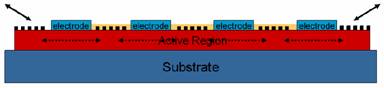
Active optical filters have been proposed a handful of times over the past decade. However, most of the proposed structures (cleaved coupled cavity based structures, and erbium doped fiber Bragg grating structures) suffer from fabrication and operational difficulties. The grating-coupled structures proposed herein are a versatile, robust technology that ensures ease of fabrication and also are ideal for implementing an active lattice filter because they are robust and highly manufacturable. The electrodes of the active lattice filter (ALF) PIC in Fig. 1 provide delay and adjustable gain. The amount of gain provided to the signals in each stage is determined by the injection current applied to the electrode. The gains control the positions of the poles and zeroes of the transfer function, and hence the magnitude and phase response of the filter. This current may be changed in a nanosecond, therefore the filter response may be changed at GHz rates. Light can be coupled into and out of the device using grating structures that are photolithographically etched on the surface. Surface gratings are also used to control the transmission and reflection between the gain sections.
|
|
|
Fig 1. GSE active lattice filter schematic. |
Two Dimensional ALF-PICs
In a traditional lattice filter, the flow of signals is forward and backward in one dimension. At the interfaces between stages, or layers, these forward and backward signals combine, with different relevant phases for different frequency components. This delay and superposition action provides for a very rich Infinite Impulse Response (IIR) filter. However, the ALF-PIC allows a two dimensional flow of signals that is unique.
|
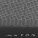
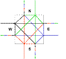
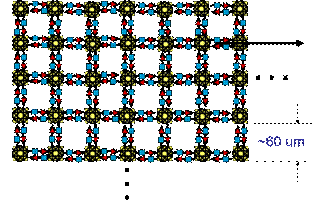
To realize the two dimensional ALF-PIC, the coupling gratings are holographicaly written in a crossed manner (Fig.2) allowing for a sophisticated signal flow that leads to a more effective and more versatile filter. The North, South, East and West flow of signals at this crossed grating junction is shown in Fig. 3 along with a two dimensional ALF. For reference, the size of a gain/delay block and a crossed grating is shown to be approximately 60 mm, although this dimension may be designed to be smaller or larger as needed. Besides Infinite Impulse Response (IIR) filters, Finite Impulse Response (FIR) filters can realized in 2D ALFs. These 2D ALFs are tunable, allow multiple inputs and outputs, and can have their response reprogrammed in approximately one nanosecond. |
|
|
|
|
Fig. 2. SEM of crossed grating, a basic building block of the 2-D Active Lattice Filter. | |
The combination of programmability and ease of manufacture provides the optical equivalent of a Field Programmable Gate Array (FPGA). FPGA economics are extremely attractive because a standardized device can be leveraged across a host of custom, even niche, applications. The development cost can be amortized across a large number of markets, providing economies of scale that are unique in the photonics world. Some preliminary theoretical results for a 2x2 lattice filter operated as a bandpass filter are shown in Fig. 4. The quality factor of the bandpass response is approximately 75,000 which is adequate for the current generation of ITU grid DWDM fiber optic communications systems. The surface plot shows that the position of the filter peak (depicted along the z-axis) may be shifted by adjusting the gains (the G's along the x- and y-axes) in each section. These plots show that for a typical design, adjusting the drive current by ~2 mA yields a tunability of approximately 20GHz. Filters of higher grade will support increased tunability and more sophisticated filter outputs.
|
|
|
|
Fig. 3. Two dimensional signal flow in a crossed surface grating and the two dimensional lattice filter that is enabled. |
|
Channels and sets of channels may be routed, added, dropped, and monitored for signal quality with this ALF. Other telecommunications applications include optical pulse reshaping, regeneration and retiming (2R/3R) and dispersion compensation. A tunable dispersion compensator would ease installation, enable OC768 (40Gbps) data rates and line side switching, in a package that is 100 times smaller than current, non-tunable dispersion compensators. Cost would be reduced by a factor of 2-3.
|
|
|
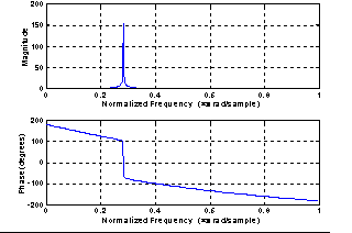
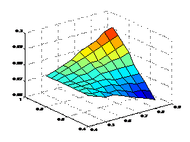
Fig. 4. Predicted behavior and gain tuning from a tunable two-dimensional GSE active lattice filter.
We have identified three key challenges in which significant progress must be made to fully accomplish our vision:
1) Photonic Integrated Circuits require integrated isolators. Although there have been initial demonstrations of such devices [20], they have extremely high insertion losses requiring an amplifier resulting in severe noise penalties. Using a reasonant-layer effect (RLE) and ferromagnetic nanoparticles, an isolator that can be integrated with InP photonic components is expected to provide 30 dB of isolation with an insertion loss of 3 dB [21].
2) Unlike the traditional lattice structure, the theoretical description of a two-dimensional lattice filter is a previously unstudied structure. While progress has been made, the full elucidation of the signal flow, stability and the design of the transfer functions must be advanced for our vision to succeed.
3) The operational range of the active optical filter will be bounded on the one side by the noise figure, a parameter that is heavily influenced by the coupling into the device. Hence the development of very high efficiency I/O couplers will greatly improve the operational performance of the PIC.
We have identified eleven milestones that we will use to track our progress towards our major goal of a real time programmable ALF PIC. Figure 5 shows this technological roadmap. The first row shows the progression of the maturity of the PIC technology culminating in the demonstration of a real-time (nanosecond reconfigurable) active lattice filter implementation. The second row of the figure represents the device demonstrations (green boxes) and nanoscience achievements (yellow boxes) which flow into the Active Lattice Filter demonstrator. The third row of the figure represents the DSP modeling effort undertaken to analyze and map architectures onto the ALF. Specific applications from this network centric vision will be mapped onto the 2-D Active Lattice Filter to demonstrate its flexibility.
|
|
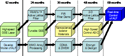
Fig. 5. Incremental demonstrator milestones culminating in the capstone demonstrator of an ALF.