Grating-Outcoupled Surface-Emitting Lasers
- Two-Wavelength GSE lasers
- Integration of GSE lasers with Heterostructure Bipolar Transistors
- Four-Wavelength GSE lasers
- High-Speed Phase-Shift Modulators for GSE lasers
- Quantum Well Intermixing
- High Power Grating-Outcoupled Surface-Emitting Lasers
Grating-Assisted Directional Couplers
 |
Southern Methodist University |
| School of Engineering | |
| Link to Dallas LEOS Section | Department of Electrical Engineering |
Quantum-Well Intermixing
The ability to control the quantum well bandgap across a III-V semiconductor laser wafer is useful for the fabrication of monolithic photonic integrated circuits (PIC's). The absorption band edge of quantum-well (QW) structures can be achieved by selective epitaxial growth, etching and regrowth or by postgrowth quantum-well intermixing (QWI) techniques, such as impurity-induced disordering (IID), photoabsorption-induced disordering (PAID) and impurity-free vacancy disordering (IFVD) [13,14]. QWI using the IFVD technique is a versatile way of controlling the bandgap of the QW after growth and has been reported for the AlGaInAs/InP material system [14] used for the proposed GSE laser. Initial results at reproducing QWI at Agilent and SMU, based on the work in [14] is shown in Fig. 14a, for QW structures that had either an InGaAs or InP final layer. Another promising approach is the use of spin-on dopants, shown in Fig. 14b[15]. Both of these approaches will be pursued on this program.
|
(a) |
(b) |
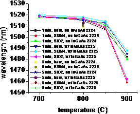
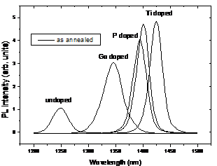
Fig. 14. a) photoluminescence shifts of AlGaInAs quantum wells as a function of temperature for SiO2 and Si3N4 capping layers; b) photoluminescence shifts of InGaAs capped InP/InGaAs quantum wells coated with an undoped, Ga-, P- or Ti- doped spin-on glasses, baked at 300C for 15 minutes and then annealed at 800C for 60s[15].