Grating-Outcoupled Surface-Emitting Lasers
- Two-Wavelength GSE lasers
- Integration of GSE lasers with Heterostructure Bipolar Transistors
- Four-Wavelength GSE lasers
- High-Speed Phase-Shift Modulators for GSE lasers
- Quantum Well Intermixing
- High Power Grating-Outcoupled Surface-Emitting Lasers
Grating-Assisted Directional Couplers
 |
Southern Methodist University |
| School of Engineering | |
| Link to Dallas LEOS Section | Department of Electrical Engineering |
Integration of GSE lasers with Heterostructure Bipolar Transistors
Successful monolithic integration of receiver modules for high speed and high performance applications include PIN Photodetectors (PD) with Transimpedance Amplifiers (TIA's) where the electronic circuits are fabricated based on High Electron Mobility Transistors (HEMTs) or Heterojunction Bipolar Transistors (HBTs) [11]. Commercial InP houses such as Vitesse, TriQuint and VSK Photonics are also pursuing monolithic integration of a PIN PD with HBT. Up to now, the merging of semiconductor lasers and laser driver electronics onto the same substrate has not yet been addressed seriously, in part due to the divergent development paths taken by optoelectronics and electronics research groups.
InP-based epitaxy materials for 1310 and 1550 nm edge emitting (EE) lasers have mostly been developed by Metal Organic Chemical Vapor Deposition (MOCVD), while the high-speed laser drivers, especially for OC-768 and beyond, are developed by Molecular Beam Epitaxy (MBE). The following are key issues difficulties for integrating the lasers and electronic drivers:
-
substrate incompatibility: n+ InP for EE Laser, and semi-insulating InP for high-speed electronic driver.
- Incompatible growth technology from the early development days: MBE and MOCVD.
- difficulty of integrating EE lasers and long-wavelength VCSELs (~14 um of epitaxy) with electronics
With the availability of the phosphorous valved cracker and other advances, MBE is now able to grow quality long wavelength InP-based lasers with the advantage of high doping and no issues with hydrogen passivation.
The objective of this task is to demonstrate a pathway for economical integration of long wavelength lasers with HBT based electronic laser drivers as shown conceptually in Fig. 11. SMU and IntelliEPI will develop a combined epitaxy structure that will add a long wavelength diode laser to an InP HBT epi structure that will serve as a basis for the development of a high performance monolithic integrated laser module. The HBT part of the epi structure will be developed based on the already well-established repertoire of HBT know-how at IntelliEPI. The long wavelength laser part will be the Grating-out-coupled Surface Emitting (GSE) semiconductor lasers developed at SMU. To verify the integrity of the combined epi structure, measurements of resulting devices will be compared to traditional HBTs and lasers. These tests will include a) large area device processing results from the HBT materials, and b) broad area laser processing results form the laser materials. As a proof of concept with successful epi materials development, an Electronic-Photonic Integrated Circuit (EPIC) consisting of a laser connected to an HBT laser driver from the same epi wafer will be fabricated.
|
|
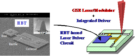
Fig. 11. A monolithic EPIC for laser module integrating both GSE laser/Modulator and HBT electronic driver [12].
|
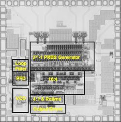
With the relative maturity of the InP HBT technology, digital, analog, and mixed signal electronic circuits at both 10 GHz and 40 GHz are now commercially available from several foundries. An InP mixed signal circuit at 43 GHz containing ~ 5000 transistors on MBE grown material from IntelliEPI is shown in Fig. 12. This work will leverage off existing and well-developed electronic InP-based HBT technology where epi materials are routinely grown on 4¡± semi-insulating substrates. The proposed EPIC, containing an HBT and a phase-shift modulated GSE, will be developed based on a single epi growth, which stacks an HBT and GSE Laser on top of each other as shown in Fig. 13. Combining both together on the same circuit will dramatically simplify device/circuit processing and down-stream module packaging. Higher speed and greater performance device/circuit will be possible. |
|
|
Fig. 12. World's highest integration of an InP based IC. A mixed signal circuit at 43 GHz fabricated from IntelliEPI InP HBT materials. (Courtesy of Vitesse Semiconductor Corporation) |
|
(a) |
(b) |
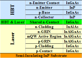
Fig. 13. a) Schematic diagram of Combined Laser + HBT with Laser on top, and b) with Laser on the bottom.